SNVAA31 November 2021 LM61435-Q1 , LM61440-Q1 , LM61460-Q1 , LM62435-Q1 , LM62440-Q1
1 LM61440-Q1 vs LM62440-Q1 Device Differences
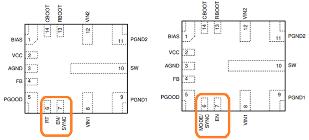
 Figure 1-1 LM61440-Q1 Pinout (Left) and LM62440-Q1 Pinout (Right)
Figure 1-1 highlights the key differences in device pin-out between the LM614xx and LM624xx device set using the LM61440-Q1 and LM62440-Q1 as device examples.
The primary distinctions between the LM614xx and LM624xx are listed below:
- Switching frequency: The LM624xx is internally set to a default switching frequency of 2.1MHz. The LM614xx enables control of the switching frequency through an adjustable RT resistor.
- Mode selection: The LM624xx enables control of the mode operation at light load. Pulling MODE/SYNC high results in FPWM mode setting while pulling MODE/SYNC low results in Auto mode setting. The LM614xx has the mode feature factory set and fixed per device option.
- External synchronization: To synchronize to a desired switching frequency the LM624xx requires a valid switching signal into the “MODE/SYNC” (Pin 6) for synchronization while the LM614xx uses “EN/SYNC” (Pin 7) for synchronization. Note that when using the external synchronization feature of the device spread-spectrum is disabled.
- Output voltage setting: The LM624xx is available in both adjustable and fixed output options. The LM614xx is only available in adjustable output option. For adjustable output options a top and bottom resistor is required while for fixed output options the feedback pin can be tied directly to the output rail for proper regulation.
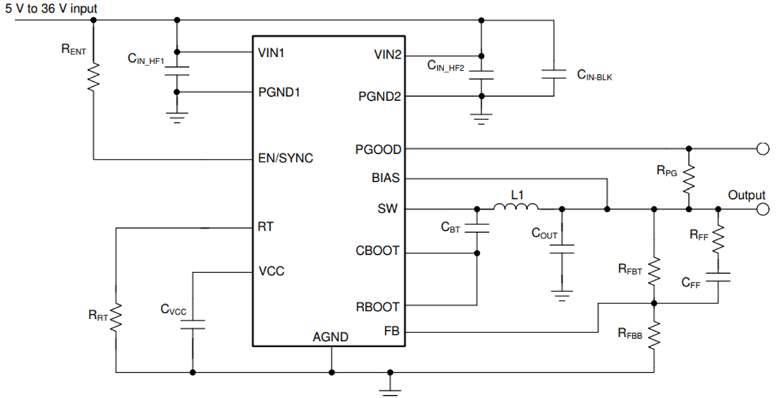
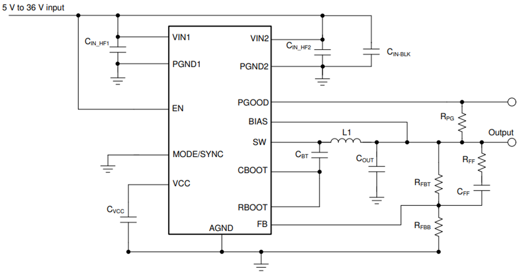
Table 1-1 and Table 1-2 show the device comparison table of the LM61440-Q1 and LM62440-Q1 example devices and illustrates the difference between a LM614xx and LM624xx. The table provides the orderable device numbers and details the variety of different options the device is factory set to. Figure 1-2 and Figure 1-3 are example application circuits from the data sheet. To create a universal footprint to interchange between the LM614xx and LM624xx device set, several components must be considered.
| DEVICE | ORDERABLE PART NUMBER | REFERENCE PART NUMBER | LIGHT LOAD MODE | SPREAD SPECTRUM | OUTPUT VOLTAGE | SWITCHING FREQUENCY |
|---|---|---|---|---|---|---|
| LM61440-Q1 | LM61440AANQRJRRQ1 | LM61440AAN-Q1 | Auto Mode | No | Adjustable | Adjustable |
| LM61440AASQRJRRQ1 | LM61440AAS-Q1 | Auto Mode | Yes | Adjustable | Adjustable | |
| LM61440AFSQRJRRQ1 | LM61440AFS-Q1 | FPWM | Yes | Adjustable | Adjustable |
| DEVICE | ORDERABLE PART NUMBER | REFERENCE PART NUMBER | LIGHT LOAD MODE | SPREAD SPECTRUM | OUTPUT VOLTAGE | SWITCHING FREQUENCY |
|---|---|---|---|---|---|---|
| LM62440-Q1 | LM62440APPQRJRRQ1 | LM62440APP-Q1 | Pin Selectable | Pin Selectable | Adjustable | 2.1 MHz |
| LM62440BPPQRJRRQ1 | LM62440BPP-Q1 | Pin Selectable | Pin Selectable | 3.3 V | 2.1 MHz | |
| LM62440CPPQRJRRQ1 | LM62440CPP-Q1 | Pin Selectable | Pin Selectable | 5 V | 2.1 MHz |
 Figure 1-2 LM61440-Q1 Example Application Circuit
 Figure 1-3 LM62440-Q1 Example Application Circuit