SNVAA63 March 2023 TPSM365R6
2.1 Additional Bypass Capacitor and Schottky Diode
You can use a ceramic bypass capacitor, CBYP, with a minimum capacitance of 10 µF, to decrease incoming power supply noise. The voltage rating of CBYP must be taken into consideration because this capacitor will experience stress equal to the full voltage range between VIN and –VOUT. In general, use a capacitor with at least twice the voltage rating of the full expected voltage range.
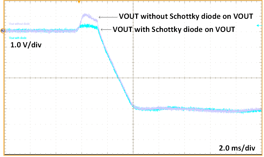
However, the inclusion of the CBYP capacitor introduces an AC path from VIN to –VOUT and might worsen the transient response. When VIN is applied to the circuit, the dV/dt across the bypass capacitor creates a current that must return to ground to complete the loop. This current might flow through the internal low-side body diode of the MOSFET and the inductor to return to ground. TI recommends having a Schottky diode between the -VOUT and SYS_GND to avoid damaging the aforementioned internal low-side MOSFET. Additionally, this Schottky diode will reduce the potential positive output voltage spike at –VOUT caused by a quick VIN startup as shown in Figure 2-2. If large line transients are expected, increase the output capacitance to keep the output voltage within acceptable levels.
Note that for the system to be stable, there must be an input power supply capacitor to help dampen the high-frequency noise that can couple into the circuit. Adding an electrolytic capacitor, CBULK, with moderate ESR can help dampen any input supply ringing caused by long power leads. This CBULK capacitor should be added across VIN and SYS_GND.
 Figure 2-2 TPSM365R6 IBB Startup with Schottky Diode