SNVAA63 March 2023 TPSM365R6
4 Typical Performance
Figure 4-1 Basic Schematic
Used
Figure 4-3 Efficiency vs. Load
Current at VIN = 24 V
Figure 4-5 Start-up on VIN
= 24 V, VOUT = –12 V, Expected Performance With no Level
Shifters
Figure 4-7 Load Transient Response,
100 mA to 410 mA With VIN = 24 V, VOUT = –12 V
Figure 4-9 Output Voltage Ripple,
VIN = 24 V, VOUT = –12 V, IOUT = 0
mA
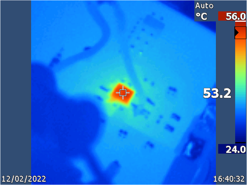
 Figure 4-11 Temperature Response,
VIN = 24 V, VOUT = –5 V, IOUT = 450
mA
| DSGNR | Part Number | Description | MFR | QTY |
|---|---|---|---|---|
| CIN | C3225X7R2A225K230AM | 2.2 uF, 100 V, X7R, 1210 | TDK | 1 |
| GRM188R72A104KA35J | 0.1 uF, 100 V, X7R, 0603 | MuRata | 1 | |
| CFF | CGA2B2C0G1H100D050BA | 10 pF, 50 V, C0G/NP0, 0402 | TDK | 1 |
| CBYP | C3225X7R2A225K230AB | 2.2 uF, 100 V, X7R, 1210 | TDK | 1 |
| CVCC | C1608X7R1C105K080AC | 1 uF, 16 V, X7R, 0603 | TDK | 1 |
| COUT | C3225X7R1E226M250AB | 22 uF, 25 V, X7R, 1210 | TDK | 2 |
Figure 4-4 Load Regulation at
VIN = 24 V
Figure 4-6 Shutdown on VIN
= 24 V, VOUT = –12 V, Expected Performance With no Level
Shifters
Figure 4-8 Load Transient Response, 0
mA to 410 mA With VIN = 24 V, VOUT = –12 V
Figure 4-10 Output Voltage Ripple,
VIN = 24 V, VOUT = –12 V, IOUT = 410
mA
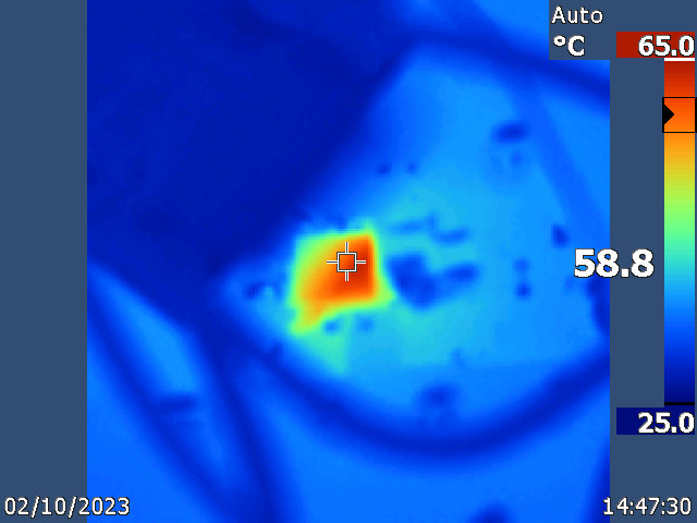
 Figure 4-12 Temperature Response,
VIN = 24 V, VOUT = –12 V, IOUT = 410
mA