SNVAA93 December 2023 LM65645-Q1 , LM70660 , LM706A0 , LM706A0-Q1 , LM70840 , LM70840-Q1 , LM70860 , LM70860-Q1 , LM70880 , LM70880-Q1 , LMR38020-Q1 , LMR38025-Q1
3.3 Power Inductor Consideration
When selecting a power inductor, it is important to consider the electrical coupling caused by the SW node through parasitic capacitance to ground. These near-field couplings can result in high-frequency EMI noise.
To mitigate this noise, the recommendation is to use an inductor with terminations positioned underneath the package. This configuration helps to minimize magnetic coupling. Additionally, the size of the inductor needs to be kept as small as possible while still meeting the requirements for Isat and Irms. This smaller size helps in minimizing the electrical coupling.
Figure 3-12 depicts two different sizes of inductors on the same board. In Figure 3-13 and Figure 3-18, the EMI test results are compared, showing that the noise level of the small-sized inductors is 5dB lower than that of the normal-sized inductor in the FM band. This demonstrates the effectiveness of using smaller-sized inductors in reducing EMI noise.
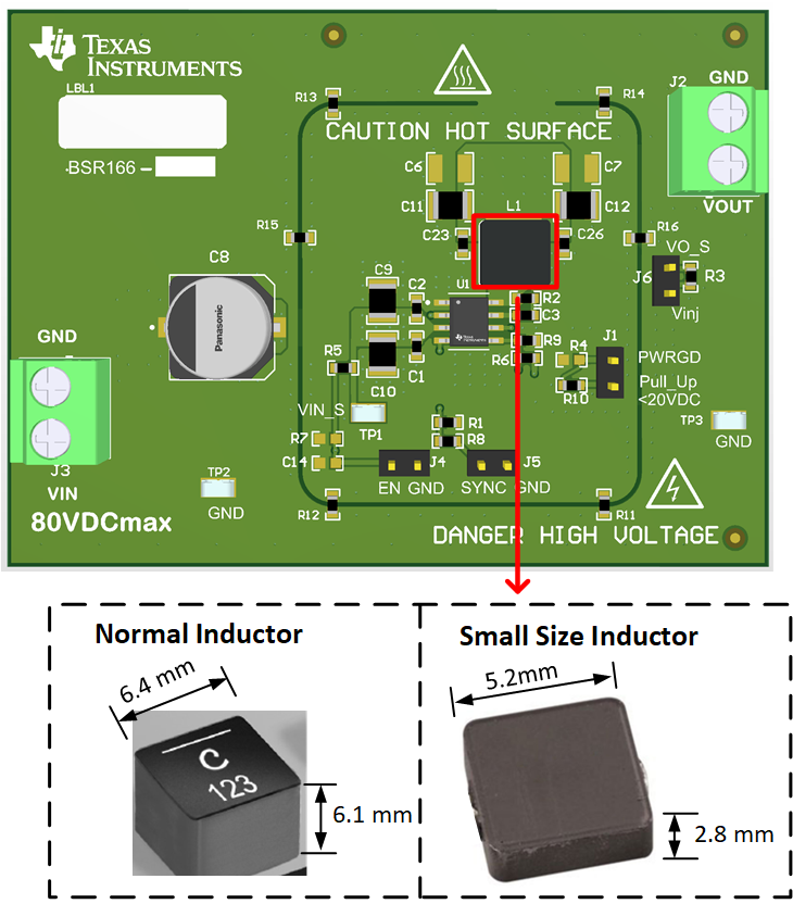 Figure 3-12 Different Size of Inductor Selection in Buck Converter
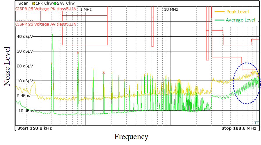 Figure 3-13 Conducted EMI Test Result
of Normal Inductor
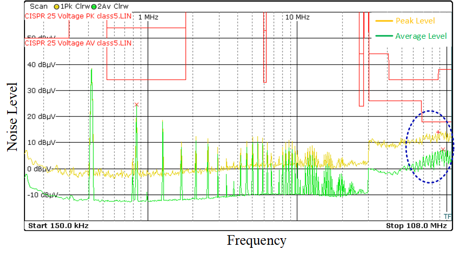 Figure 3-14 Conducted EMI Test Result
of Small Size Inductor
Figure 3-14 Conducted EMI Test Result
of Small Size InductorAdding a shield is a commonly used method to reduce EMI noise. The shield needs to be connected to the PCB ground to effectively mitigate noise. Figure 3-15 illustrates the impact of adding a shield. The parasitic capacitance Cp between the SW node and ground is replaced by two capacitance: Cp1, which represents the capacitance between the SW node and PCB ground, and Cp2, which represents the capacitance between the PCB ground and the overall ground. The CM noise emission model, as shown in Figure 3-22, also changes when a shield is added. The CM noise now flows between Cp1 and the PCB ground, rather than flowing into chassis (system) ground. This change in noise flow can make the noise less detectable by the LISN.
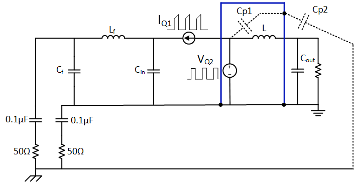 Figure 3-15 The Shield Effect on Parasitic
Capacitance
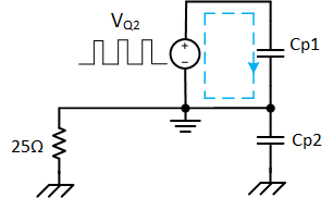 Figure 3-16 CM Noise Emission Model of
Shield Added
Figure 3-16 CM Noise Emission Model of
Shield AddedTraditional shields are often bulky and have poor heat dissipation. To overcome these limitations, selecting an inductor with a metal shield can be a better option. Figure 3-25 presents the test results of using a metal shield inductor. It can be observed that compared to the normal inductor noise shown in Figure 3-13, the EMI noise in the FM band is reduced by approximately 10dB when using the metal shield inductor. This demonstrates the effectiveness of using a metal shield inductor in reducing EMI noise.
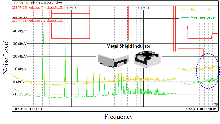 Figure 3-17 Conducted EMI Result of Metal
Shield Inductor