SNVAA93 December 2023 LM65645-Q1 , LM70660 , LM706A0 , LM706A0-Q1 , LM70840 , LM70840-Q1 , LM70860 , LM70860-Q1 , LM70880 , LM70880-Q1 , LMR38020-Q1 , LMR38025-Q1
3.2 Layout Consideration
Layout plays a crucial role in minimizing EMI noise, and when possible, a four-layer PCB is recommended. The top layer should primarily accommodate the converter, inductor, and SW node, all of which are noise sources. The second layer should be a continuous copper pour acting as a ground plane to provide shielding. The third layer can be utilized for routing input, output, and signal traces. Lastly, the bottom layer should house the EMI filter, positioned far away from the noise sources on the top layer.
The recommended layout for the synchronous buck converter LMR38020-Q1 is outlined below, with important points to consider:
- Top-layer considerations, as shown in Figure 3-5.
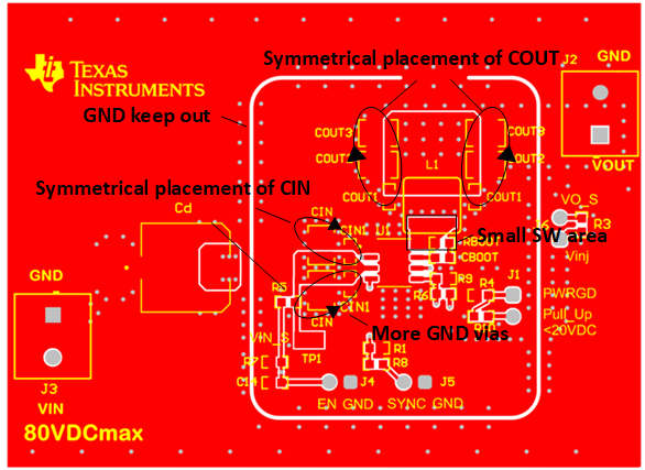 Figure 3-5 Top-layer Layout
- The input capacitor (Cin) should be positioned in close proximity to the VIN and GND pins to minimize the input-critical loop area. Additionally, more vias should be placed around the GND and VIN planes of Cin to reduce the parasitic inductance of the input current loop. Moreover, Cin should be placed symmetrically to create two input loops, which cancels out the magnetic field induced and weakens magnetic coupling to the LISN. Similarly, the output capacitor should also be placed symmetrically to achieve the same effect.
- The SW node, being a major source of noise, should be routed without any vias connected to other layers. Furthermore, the SW node area should be kept small to minimize the parasitic capacitor (Cp).
- It is advisable to include a GND keep out area to isolate the outer GND from the inner GND noise.
Figure 3-6 illustrates the placement of Cin in both asymmetric and symmetrical configurations. Figure 3-13 and Figure 3-13 display the comparison of EMI test results between the two configurations. The data indicates that in the FM band, the peak and average noise levels of the symmetrical capacitor placement are approximately 4dB lower compared to the asymmetric configuration. This finding validates the benefits of magnetic field cancellation achieved through the symmetrical placement of capacitors.
 Figure 3-6 Cin With and Without Symmetrical Placement of Buck Converter
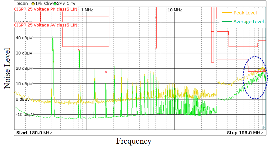 Figure 3-7 Conducted EMI Test Result of Non-symmetrical Cin Placement
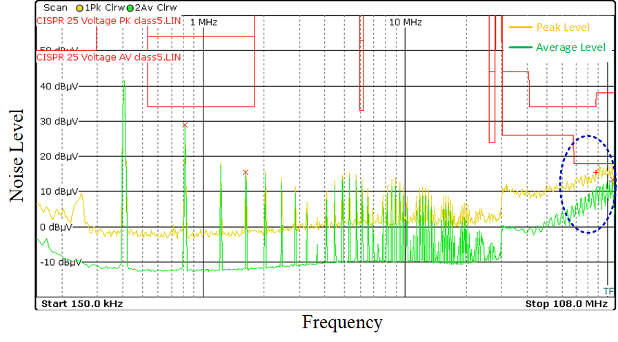 Figure 3-8 Conducted EMI Test Result of Symmetrical Cin Placement
Figure 3-25 demonstrates the second layer layout considerations. In this layout the entire second layer is filled with copper as the ground plane. This ground plane is positioned directly underneath the input critical loop and the inductor. By doing so, eddy currents are induced in the copper which help weaken the magnetic coupling between components and reduces the overall EMI noise.
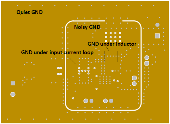 Figure 3-9 Second-layer Layout
- Third-layer is shown in Figure 3-22, this layer is mainly used for signal traces. Signals such as PowerGood and EN UVLO can be routed on this plane.
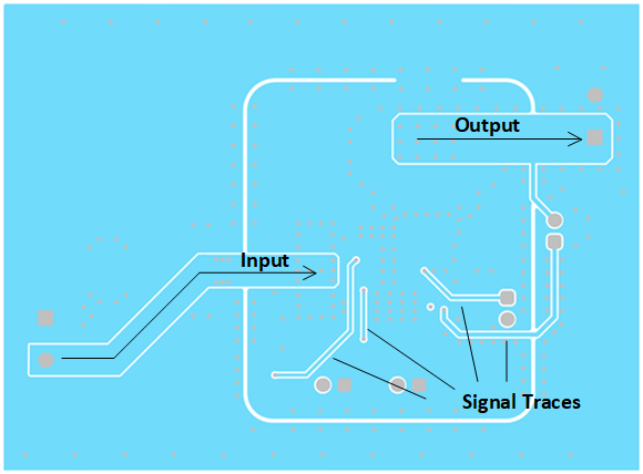 Figure 3-10 Third-layer Layout
 - Bottom-layer is shown in Figure 3-12. The EMI filter is placed on this layer and away from the noise sources previously discussed that are on top layer. Notice the filter capacitors are placed symmetrically as well to further reduce any magnetic coupling.
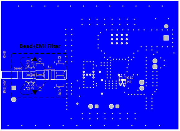 Figure 3-11 Bottom-layer Layout