SNVSA77D December 2015 – November 2016 LP5912
PRODUCTION DATA.
- 1 Features
- 2 Applications
- 3 Description
- 4 Revision History
- 5 Voltage Options
- 6 Pin Configuration and Functions
- 7 Specifications
- 8 Typical Characteristics
- 9 Detailed Description
- 10Applications and Implementation
- 11Power Supply Recommendations
- 12Layout
- 13Device and Documentation Support
- 14Mechanical, Packaging, and Orderable Information
9 Detailed Description
9.1 Overview
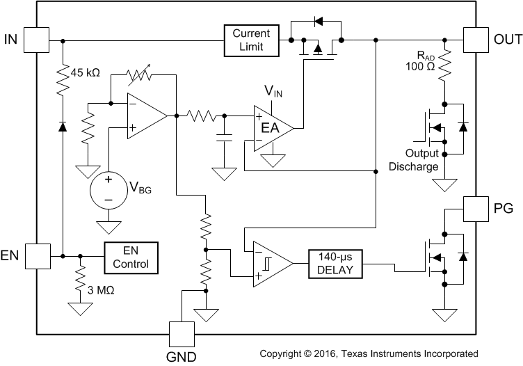
The LP5912 is a low-noise, high PSRR, LDO capable of sourcing a 500-mA load. The LP5912 can operate down to 1.6-V input voltage and 0.8-V output voltage. This combination of low noise, high PSRR, and low output voltage makes the device an ideal low dropout (LDO) regulator to power a multitude of loads from noise-sensitive communication components to battery-powered system.
The LP5912 Functional Block Diagram contains several features, including:
9.2 Functional Block Diagram

9.3 Feature Description
9.3.1 Enable (EN)
The LP5912 EN pin is internally held low by a 3-MΩ resistor to GND. The EN pin voltage must be higher than the VEN(ON) threshold to ensure that the device is fully enabled under all operating conditions. The EN pin voltage must be lower than the VEN(OFF) threshold to ensure that the device is fully disabled and the automatic output discharge is activated.
When the device is disabled the output stage is disabled, the PG output pin is low, and the output automatic discharge is ON.
9.3.2 Output Automatic Discharge (RAD)
The LP5912 output employs an internal 100-Ω (typical) pulldown resistance to discharge the output when the EN pin is low. Note that if the LP5912 EN pin is low (the device is OFF) and the OUT pin is held high by a secondary supply, current flows from the secondary supply through the automatic discharge pulldown resistor to ground.
9.3.3 Reverse Current Protection (IRO)
The LP5912 input is protected against reverse current when output voltage is higher than the input. In the event that extra output capacitance is used at the output, a power-down transient at the input would normally cause a large reverse current through a conventional regulator. The LP5912 includes a reverse voltage detector that trips when VIN drops below VOUT, shutting off the regulator and opening the PMOS body diode connection, preventing any reverse current from the OUT pin from flowing to the IN pin.
If the LP5912 EN pin is low (the LP5912 is OFF) and the OUT pin is held high by a secondary supply, current flows from the secondary supply through the automatic discharge pulldown resistor to ground. This is not reverse current, this is automatic discharge pulldown current.
Note that reverse current (IRO) is measured at the IN pin.
9.3.4 Internal Current Limit (ISC)
The internal current limit circuit is used to protect the LDO against high-load current faults or shorting events. The LDO is not designed to operate continuously at the ISC current limit. During a current-limit event, the LDO sources constant current. Therefore, the output voltage falls when load impedance decreases. Note also that if a current limit occurs and the resulting output voltage is low, excessive power may be dissipated across the LDO, resulting in a thermal shutdown of the output.
9.3.5 Thermal Overload Protection (TSD)
Thermal shutdown disables the output when the junction temperature rises to approximately 160°C, which allows the device to cool. When the junction temperature cools to approximately 145°C, the output circuitry enables. Based on power dissipation, thermal resistance, and ambient temperature, the thermal protection circuit may cycle on and off. This thermal cycling limits the dissipation of the regulator and protects it from damage as a result of overheating.
9.3.6 Power-Good Output (PG)
The LP5912 device has a power-good function that works by toggling the state of the PG output pin. When the output voltage falls below the PG threshold voltage (PGLTH), the PG pin open-drain output engages (low impedance to GND). When the output voltage rises above the PG threshold voltage (PGVHTH), the PG pin becomes high impedance. By connecting a pullup resistor to an external supply, any downstream device can receive PG as a logic signal. Make sure that the external pullup supply voltage results in a valid logic signal for the receiving device or devices. Use a pullup resistor from 10 kΩ to 100 kΩ for best results.
The input supply, VIN, must be no less than the minimum operating voltage of 1.6 V to ensure that the PG pin output status is valid. The PG pin output status is undefined when VIN is less than 1.6 V.
In power-good function, the PG output pin being pulled high is typically delayed 140 µs after the output voltage rises above the PGHTH threshold voltage. If the output voltage rises above the PGHTH threshold and then falls below the PGLTH threshold voltage the PG pin falls immediately with no delay time.
If the PG function is not needed, the pullup resistor can be eliminated, and the PG pin can be either connected to ground or left floating.
9.4 Device Functional Modes
9.4.1 Enable (EN)
The LP5912 EN pin is internally held low by a 3-MΩ resistor to GND. The EN pin voltage must be higher than the VEN(ON) threshold to ensure that the device is fully enabled under all operating conditions. When the EN pin voltage is lower than the VEN(OFF) threshold, the output stage is disabled, the PG pin goes low, and the output automatic discharge circuit is activated. Any charge on the OUT pin is discharged to ground through the internal 100-Ω (typical) output auto discharge pulldown resistance.
9.4.2 Minimum Operating Input Voltage (VIN)
The LP5912 device does not include any dedicated UVLO circuit. The device internal circuit is not fully functional until VIN is at least 1.6 V. The output voltage is not regulated until VIN has reached at least the greater of 1.6 V or (VOUT + VDO).