SNVSA77D December   2015  – November 2016 LP5912

PRODUCTION DATA.  

  1. Features
  2. Applications
  3. Description
  4. Revision History
  5. Voltage Options
  6. Pin Configuration and Functions
  7. Specifications
    1. 7.1 Absolute Maximum Ratings
    2. 7.2 ESD Ratings
    3. 7.3 Recommended Operating Conditions
    4. 7.4 Thermal Information
    5. 7.5 Electrical Characteristics
    6. 7.6 Output and Input Capacitors
  8. Typical Characteristics
  9. Detailed Description
    1. 9.1 Overview
    2. 9.2 Functional Block Diagram
    3. 9.3 Feature Description
      1. 9.3.1 Enable (EN)
      2. 9.3.2 Output Automatic Discharge (RAD)
      3. 9.3.3 Reverse Current Protection (IRO)
      4. 9.3.4 Internal Current Limit (ISC)
      5. 9.3.5 Thermal Overload Protection (TSD)
      6. 9.3.6 Power-Good Output (PG)
    4. 9.4 Device Functional Modes
      1. 9.4.1 Enable (EN)
      2. 9.4.2 Minimum Operating Input Voltage (VIN)
  10. 10Applications and Implementation
    1. 10.1 Application Information
    2. 10.2 Typical Application
      1. 10.2.1 Design Requirements
      2. 10.2.2 Detailed Design Procedure
        1. 10.2.2.1 External Capacitors
        2. 10.2.2.2 Input Capacitor
        3. 10.2.2.3 Output Capacitor
        4. 10.2.2.4 Capacitor Characteristics
        5. 10.2.2.5 Remote Capacitor Operation
        6. 10.2.2.6 Power Dissipation
        7. 10.2.2.7 Estimating Junction Temperature
      3. 10.2.3 Application Curves
  11. 11Power Supply Recommendations
  12. 12Layout
    1. 12.1 Layout Guidelines
    2. 12.2 Layout Example
  13. 13Device and Documentation Support
    1. 13.1 Related Documentation
    2. 13.2 Receiving Notification of Documentation Updates
    3. 13.3 Community Resources
    4. 13.4 Trademarks
    5. 13.5 Electrostatic Discharge Caution
    6. 13.6 Glossary
  14. 14Mechanical, Packaging, and Orderable Information

Typical Characteristics

Unless otherwise stated: VIN = VOUT + 0.5 V, VEN = VIN, IOUT = 1 mA, CIN = 1 µF, COUT = 1 µF, TJ = 25°C, unless otherwise stated.
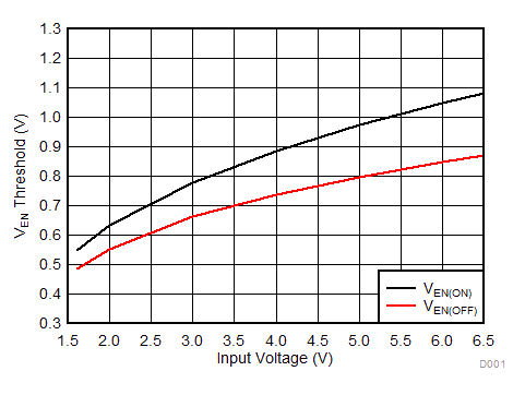
LP5912 D001_SNVSA77.gif
Figure 1. VEN Thresholds vs Input Voltage
LP5912 D003_SNVSA77.gif
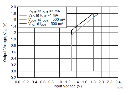
Figure 3. LP5912-1.8 Output Voltage, VPG vs Input Voltage
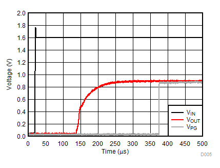
LP5912 D005_SNVSA77.gif
VIN = 0 V to 1.6 V IOUT = 1 mA
Figure 5. LP5912-0.9 Power Up
LP5912 D007_SNVSA77.gif
VIN = 0 V to 2.3 V IOUT = 1 mA
Figure 7. LP5912-1.8 Power Up
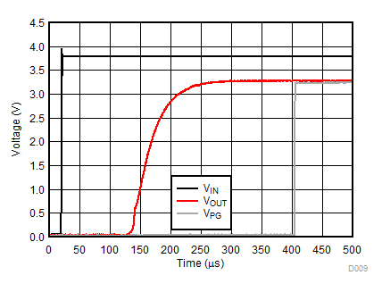
LP5912 D009_SNVSA77.gif
VIN = 0 V to 3.8 V IOUT = 1 mA
Figure 9. LP5912-3.3 Power Up
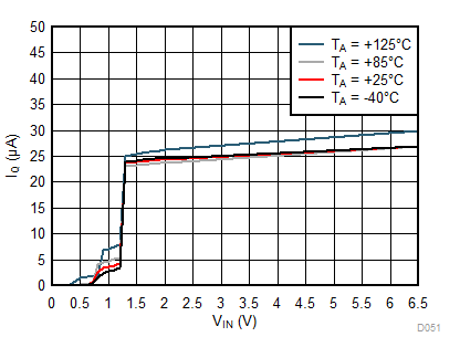
LP5912 D051_SNVSA77.gif
IOUT = 0 mA
Figure 11. LP5912-0.9 IQ (No Load) vs VIN
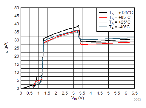
LP5912 D053_SNVSA77.gif
IOUT = 0 mA
Figure 13. LP5912-3.3 IQ (No Load) vs VIN
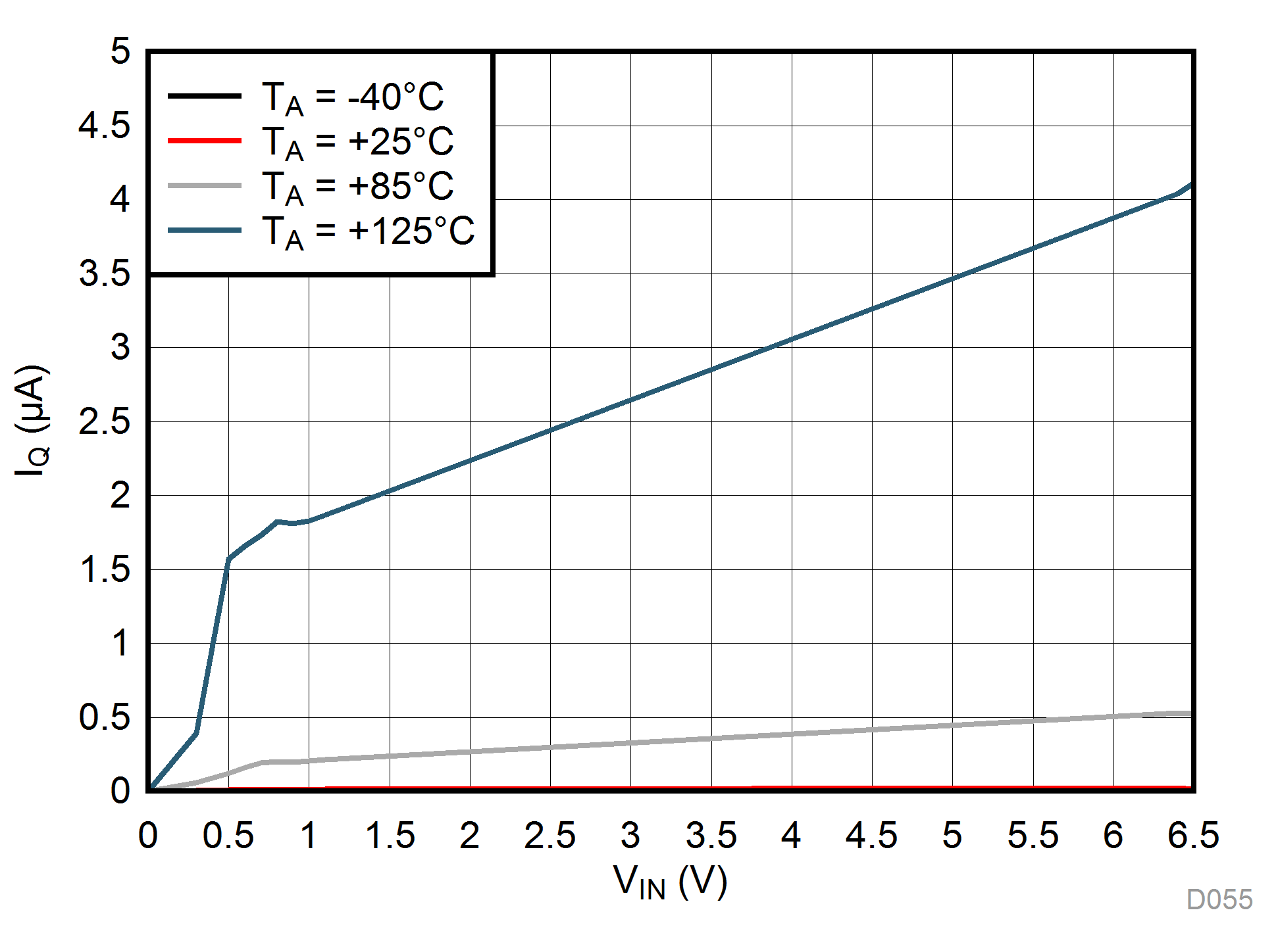
LP5912 D055_SNVSA77.png
VEN = 0 V
Figure 15. LP5912-1.8 IQ(SD) vs VIN
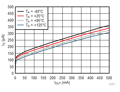
LP5912 D057_SNVSA77.gif
VIN = 1.6 V
Figure 17. LP5912-0.9 IGND vs IOUT
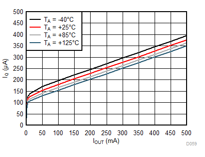
LP5912 D059_SNVSA77.gif
Figure 19. LP5912-3.3 IGND vs IOUT
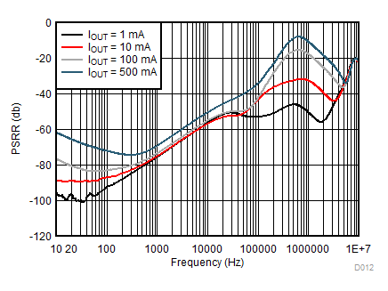
LP5912 D012_SNVSA77.gif
VIN = 1.6 V
Figure 21. LP5912-0.9 PSRR vs Frequency
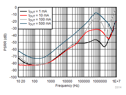
LP5912 D014_SNVSA77.gif
Figure 23. LP5912-1.8 PSRR vs Frequency
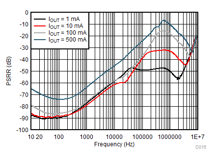
LP5912 D016_SNVSA77.gif
Figure 25. LP5912-3.3 PSRR vs Frequency
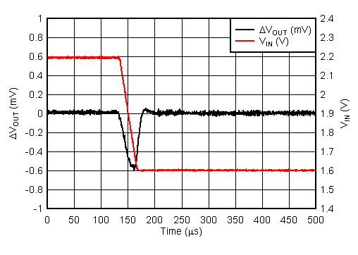
LP5912 D018_SNVSA77.gif
VIN = 2.2 V to 1.6 V tfall = 30 µs
Figure 27. LP5912-0.9 Line Transient
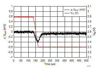
LP5912 D020_SNVSA77.gif
VIN = 2.9 V to 2.3 V tfall = 30 µs
Figure 29. LP5912-1.8 Line Transient
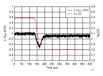
LP5912 D022_SNVSA77.gif
VIN = 4.4 V to 3.8 V tfall = 30 µs
Figure 31. LP5912-3.3 Line Transient
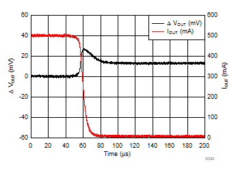
LP5912 D024_SNVSA77.gif
VIN = 1.6 V IOUT = 500 mA to 5 mA tfall = 10 µs
Figure 33. LP5912-0.9 Load Transient Response
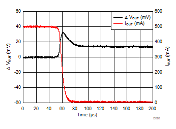
LP5912 D026_SNVSA77.gif
IOUT = 500 mA to 5 mA tfall = 10 µs
Figure 35. LP5912-1.8 Load Transient Response
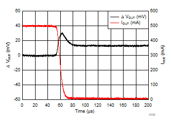
LP5912 D028_SNVSA77.gif
IOUT = 500 mA to 5 mA tfall = 10 µs
Figure 37. LP5912-3.3 Load Transient Response
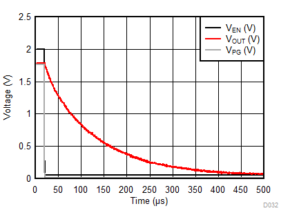
LP5912 D032_SNVSA77.gif
IOUT = 0 mA COUT = 1 µF
Figure 39. LP5912-1.8 VOUT vs VEN(OFF)
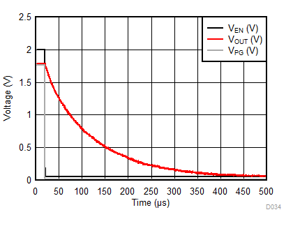
LP5912 D034_SNVSA77.gif
IOUT = 1 mA COUT = 1 µF
Figure 41. LP5912-1.8 VOUT vs VEN(OFF)
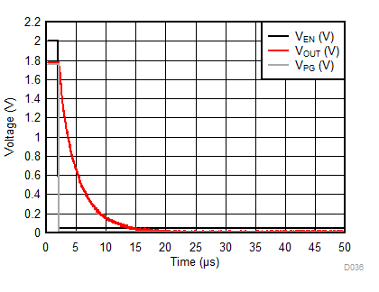
LP5912 D036_SNVSA77.gif
IOUT = 500 mA COUT = 1 µF
Figure 43. LP5912-1.8 VOUT vs VEN(OFF)
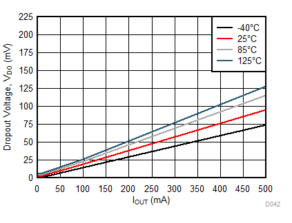
LP5912 D042_SNVSA77.gif
Figure 45. LP5912-3.3 Dropout Voltage (VDO) vs IOUT
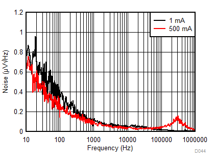
LP5912 D044_SNVSA77.gif
Figure 47. LP5912-1.8 Noise vs Frequency
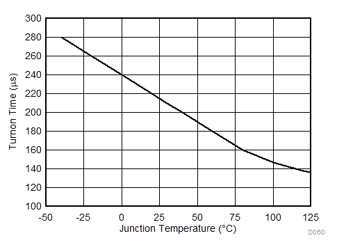
LP5912 D060_SNVSA77.gif
IOUT = 0 mA (No Load)
Figure 49. LP5912-3.3 Turnon Time vs Junction Temperature
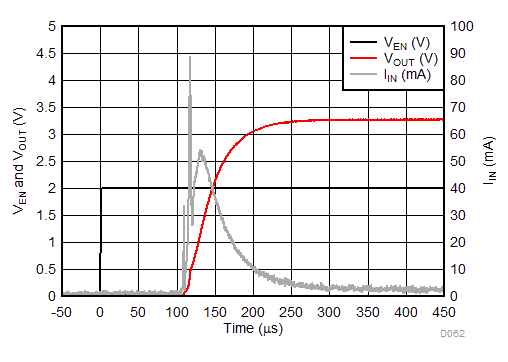
LP5912 D062_SNVSA77.gif
CIN = Open IOUT = 1 mA COUT = 1 µF
Figure 51. LP5912-3.3 In-Rush Current
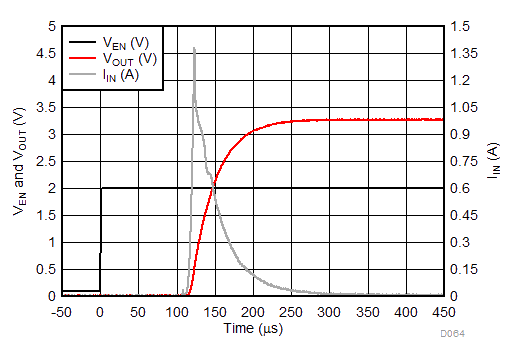
LP5912 D064_SNVSA77.gif
CIN = Open IOUT = 1 mA COUT = 10 µF
Figure 53. LP5912-3.3 In-Rush Current
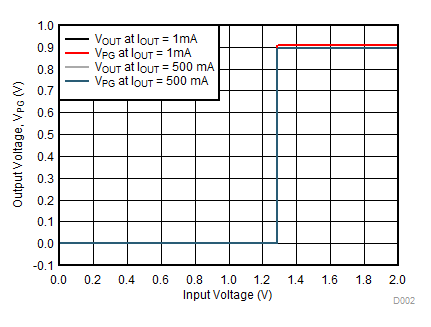
LP5912 D002_SNVSA77.gif
Figure 2. LP5912-0.9 Output Voltage, VPG vs Input Voltage
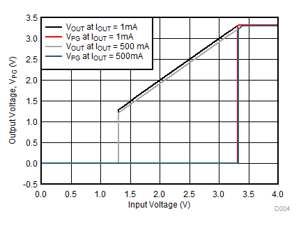
LP5912 D004_SNVSA77.gif
Figure 4. LP5912-3.3 Output Voltage, VPG vs Input Voltage
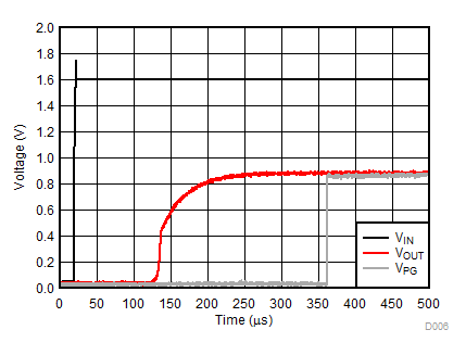
LP5912 D006_SNVSA77.gif
VIN = 0 V to 1.6 V IOUT = 500 mA
Figure 6. LP5912-0.9 Power Up
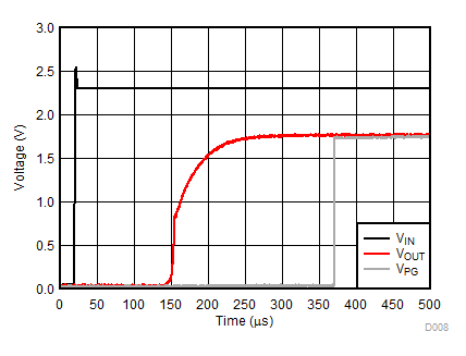
LP5912 D008_SNVSA77.gif
VIN = 0 V to 2.3 V IOUT = 500 mA
Figure 8. LP5912-1.8 Power Up
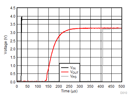
LP5912 D010_SNVSA77.gif
VIN = 0 V to 3.8 V IOUT = 500 mA
Figure 10. LP5912-3.3 Power Up
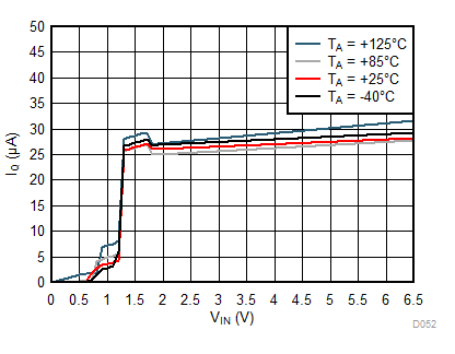
LP5912 D052_SNVSA77.gif
IOUT = 0 mA
Figure 12. LP5912-1.8 IQ (No Load) vs VIN
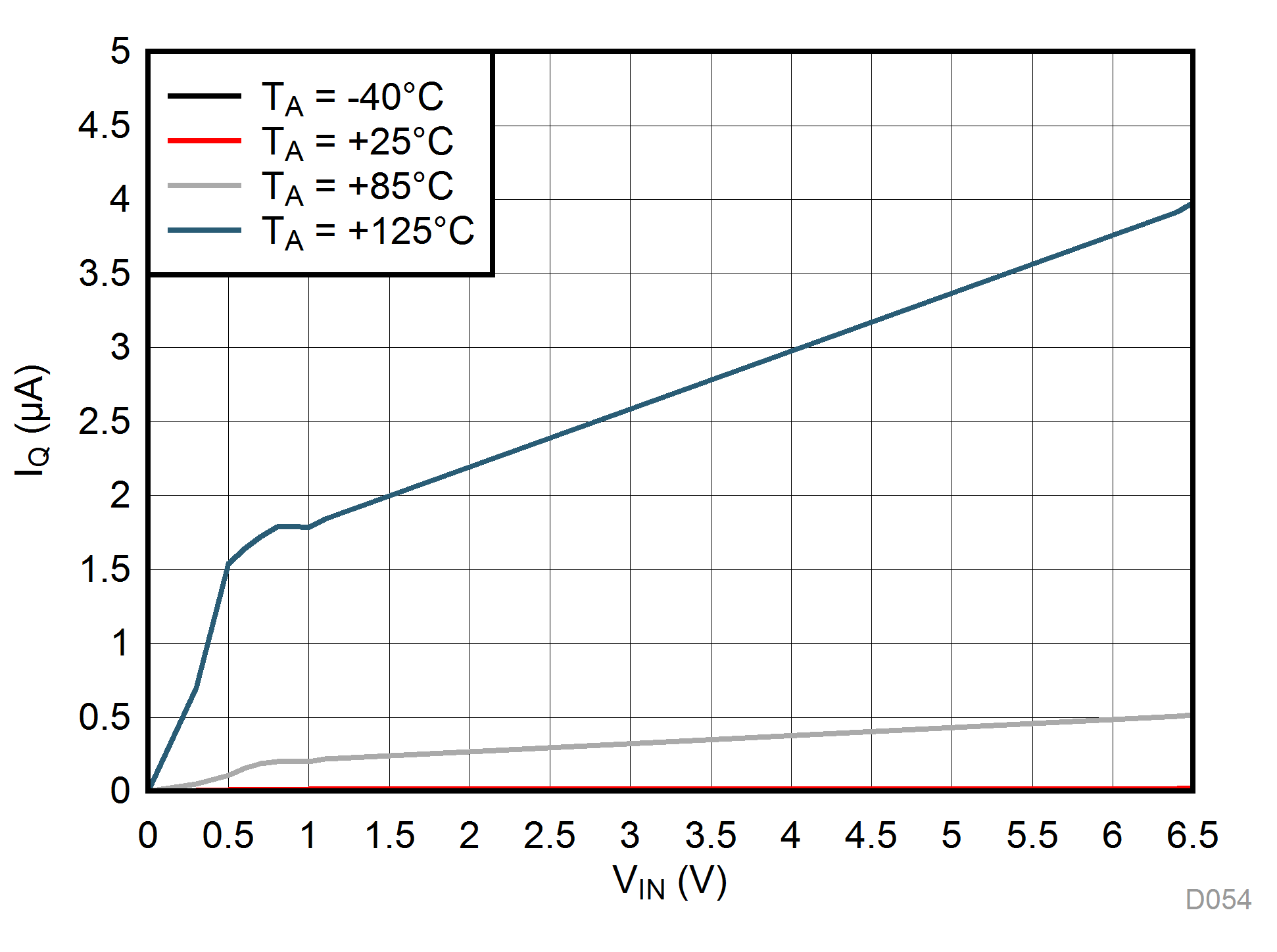
LP5912 D054_SNVSA77.png
VEN = 0 V
Figure 14. LP5912-0.9 IQ(SD) vs VIN
LP5912 D056_SNVSA77.png
VEN = 0 V
Figure 16. LP5912-3.3 IQ(SD) vs VIN
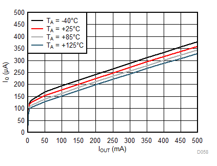
LP5912 D058_SNVSA77.gif
Figure 18. LP5912-1.8 IGND vs IOUT
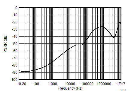
LP5912 D011_SNVSA77.gif
VIN = 1.6 V IOUT = 20 mA
Figure 20. LP5912-0.9 PSRR vs Frequency
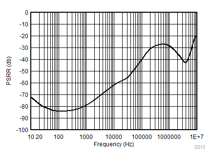
LP5912 D013_SNVSA77.gif
IOUT = 20 mA
Figure 22. LP5912-1.8 PSRR vs Frequency
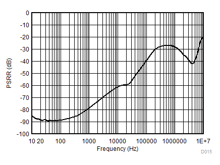
LP5912 D015_SNVSA77.gif
IOUT = 20 mA
Figure 24. LP5912-3.3 PSRR vs Frequency
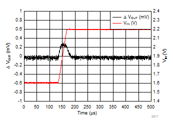
LP5912 D017_SNVSA77.gif
VIN = 1.6 V to 2.2 V trise = 30 µs
Figure 26. LP5912-0.9 Line Transient
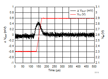
LP5912 D019_SNVSA77.gif
VIN = 2.3 V to 2.9 V trise = 30 µs
Figure 28. LP5912-1.8 Line Transient
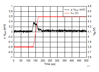
LP5912 D021_SNVSA77.gif
VIN = 3.8 V to 4.4 V trise = 30 µs
Figure 30. LP5912-3.3 Line Transient
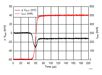
LP5912 D023_SNVSA77.gif
VIN = 1.6 V IOUT = 5 mA to 500 mA trise = 10 µs
Figure 32. LP5912-0.9 Load Transient Response
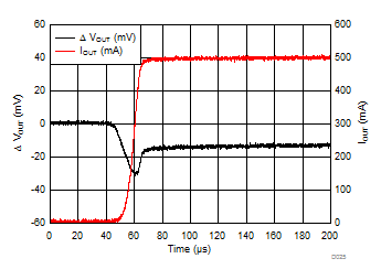
LP5912 D025_SNVSA77.gif
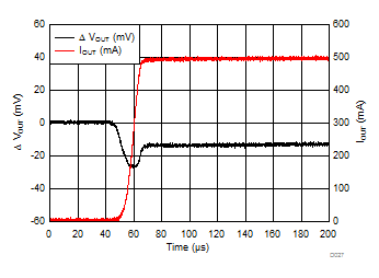
IOUT = 5 mA to 500 mA trise = 10 µs
Figure 34. LP5912-1.8 Load Transient Response
LP5912 D027_SNVSA77.gif
IOUT = 5 mA to 500 mA trise = 10 µs
Figure 36. LP5912-3.3 Load Transient Response
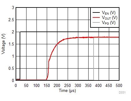
LP5912 D031_SNVSA77.gif
IOUT = 0 mA COUT = 1 µF
Figure 38. LP5912-1.8 VOUT vs VEN(ON)
LP5912 D033_SNVSA77.gif
IOUT = 1 mA COUT = 1 µF
Figure 40. LP5912-1.8 VOUT vs VEN(ON)
LP5912 D035_SNVSA77.gif
IOUT = 500 mA COUT = 1 µF
Figure 42. LP5912-1.8 VOUT vs VEN(ON)
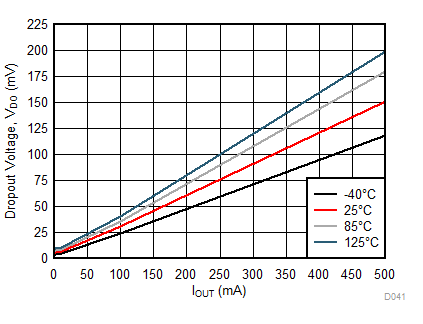
LP5912 D041_SNVSA77.gif
Figure 44. LP5912-1.8 Dropout Voltage (VDO) vs IOUT
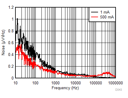
LP5912 D043_SNVSA77.gif
VIN = 1.6 V
Figure 46. LP5912-0.9 Noise vs Frequency
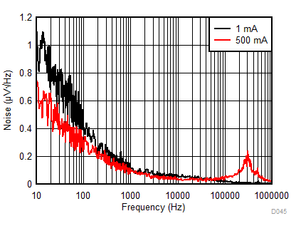
LP5912 D045_SNVSA77.gif
Figure 48. LP5912-3.3 Noise vs Frequency
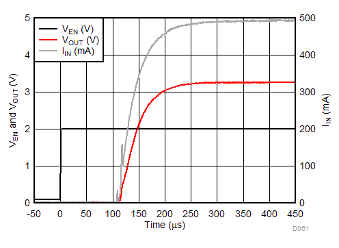
LP5912 D061_SNVSA77.gif
CIN = Open IOUT = 500 mA COUT = 1 µF
Figure 50. LP5912-3.3 In-Rush Current
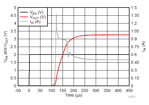
LP5912 D063_SNVSA77.gif
CIN = Open IOUT = 500 mA COUT = 10 µF
Figure 52. LP5912-3.3 In-Rush Current