SNVU863 july   2023


  1.   1
  2.   Description
  3.   3
  4.   Features
  5.   Applications
  6.   6
  7. 1Evaluation Module Overview
    1. 1.1 Introduction
    2. 1.2 Kit Contents
    3. 1.3 Specification
    4. 1.4 Device Information
  8. 2Hardware
    1.     General Texas Instruments High Voltage Evaluation (TI HV EVM) User Safety Guidelines
    2. 2.1 Test Points
      1. 2.1.1 Key Connections
        1. 2.1.1.1 Connect a Supply to J3 Connector
        2. 2.1.1.2 PWM Input
        3. 2.1.1.3 J1 Connector: Power Supply
    3. 2.2 Power-Up Procedure
      1. 2.2.1 Step 1: Driver Bias Supply
      2. 2.2.2 Step 2: Input Supply
      3. 2.2.3 Step 3: Measure SW Voltage
      4. 2.2.4 Setting Dead-Time
    4. 2.3 Power-Down Procedure
    5. 2.4 Assembly Guidelines
  9. 3Implementation Results
    1. 3.1 Electrical Performance Specifications
      1. 3.1.1 Evaluation Setup
      2. 3.1.2 Performance Data and Results
  10. 4Hardware Design Files
    1. 4.1 Schematic
    2. 4.2 PCB Layouts
    3. 4.3 Bill of Materials
  11. 5Additional Information
    1. 5.1 Trademarks

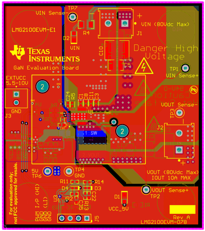
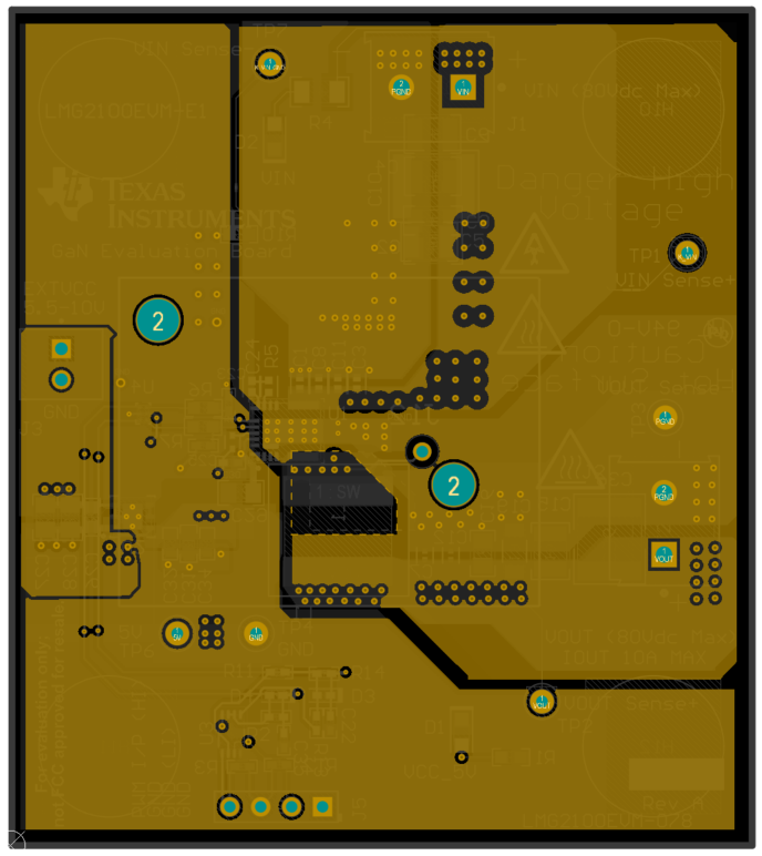
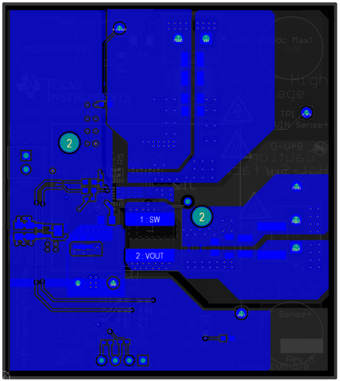
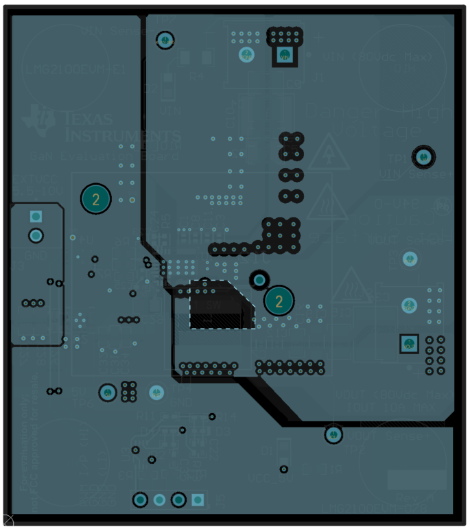
PCB Layouts

GUID-20230629-SS0I-0LRG-PXCG-DM0PSXHPXC87-low.png Figure 4-2 Top Layer of the PCB
GUID-20230629-SS0I-DMFF-JRNC-X98LTM552BSB-low.png Figure 4-3 Mid Layer-1 showing return path for power loop
GUID-20230629-SS0I-GHGL-BD4J-GQKTLHSWVMMD-low.png Figure 4-4 Mid Layer-2
GUID-20230629-SS0I-WQMQ-2TJS-SWCCCVCTNPCX-low.png Figure 4-5 Bottom Layer