SPRUIM6A October   2018  – November 2020


  1. 1Introduction
    1. 1.1 Key Features
  2. 2AM65x IDK Overview
  3. 3Common Processor Board
    1. 3.1 Key Features
    2. 3.2 Functional Block Diagram
    3. 3.3 Overview of Common Processor Board
      1. 3.3.1  Clocking
        1. 3.3.1.1 RTC Clock
        2. 3.3.1.2 Maxwell SoC Clock
        3. 3.3.1.3 Ethernet PHY Clocks
        4. 3.3.1.4 SERDES Clock
      2. 3.3.2  Reset
      3. 3.3.3  Power Requirements
        1. 3.3.3.1 Power Input
        2. 3.3.3.2 Overvoltage and Undervoltage Protection Circuit
        3. 3.3.3.3 Voltage Supervisor
        4. 3.3.3.4 Current Monitoring
        5. 3.3.3.5 Power Supply
        6. 3.3.3.6 Power Sequencing
        7. 3.3.3.7 SoC Power
      4. 3.3.4  Configuration
        1. 3.3.4.1 Boot Modes
        2. 3.3.4.2 JTAG
          1. 3.3.4.2.1 Test Automation
        3. 3.3.4.3 UART Interface
      5. 3.3.5  Memory Interfaces
        1. 3.3.5.1 DDR4 Interface
        2. 3.3.5.2 MMC Interface
          1. 3.3.5.2.1 SDHC Interface
          2. 3.3.5.2.2 eMMC Interface
        3. 3.3.5.3 OSPI Interface
        4. 3.3.5.4 SPI NOR Flash Interface
        5. 3.3.5.5 Board ID EEPROM Interface
        6. 3.3.5.6 Boot EEPROM Interface
      6. 3.3.6  Ethernet Interface
        1. 3.3.6.1 Gigabit Ethernet PHY Default Configuration
        2. 3.3.6.2 Ethernet LEDs
      7. 3.3.7  LCD Display Interface
      8. 3.3.8  USB 2.0 Interface
      9. 3.3.9  CSI-2 Interface
      10. 3.3.10 Application Card Interface
      11. 3.3.11 SERDES Interface
      12. 3.3.12 GPMC/DSS Interface
      13. 3.3.13 I2C Interface
      14. 3.3.14 SPI Interface
      15. 3.3.15 Timer and Interrupt
        1. 3.3.15.1 Timer
        2. 3.3.15.2 Interrupt
      16. 3.3.16 Fan Connector
  4. 4IDK Application Card
    1. 4.1 Key Features
    2. 4.2 Overview of IDK Application Board
      1. 4.2.1 Application Card Connector
      2. 4.2.2 Profibus Interface
      3. 4.2.3 CAN Interface
      4. 4.2.4 Rotary Switch
      5. 4.2.5 Industrial I/O Terminal Connector
      6. 4.2.6 Ethernet Interface
      7. 4.2.7 Board ID Memory
      8. 4.2.8 Power Supply
  5. 5x2 Lane PCIe Personality Card
    1. 5.1 Key Features
    2. 5.2 Overview of PCIex2 Daughter Card
      1. 5.2.1 Personality Card Connectors
      2. 5.2.2 USB 2.0 Interface
      3. 5.2.3 PCIe Interface
      4. 5.2.4 x2 Lane PCIe Personality Card Clocking
      5. 5.2.5 Board ID EEPROM Interface
      6. 5.2.6 x2 Lane PCIe Personality Card Power
  6. 6Known Issues
    1. 6.1 Determining the Revision and Date Code for the EVM
    2. 6.2 Known Issues for the A, E4, and E3 Revision
      1. 6.2.1 Lack of Reset for I2C IO Expander
    3. 6.3 Known Issues for the E4 & E3 Revision
      1. 6.3.1 Changes Unique to the E4 Revision Modified for 2.0 Revision
    4. 6.4 Known Issues for the E3 Revision
      1. 6.4.1 Resonance Observed on the SoC Side of Some Filters Associated with VDDA_1V8
      2. 6.4.2 Additional LDO Power Supply Needed for VDDA_1P8_SERDES0
      3. 6.4.3 Length of the RESET Signal to the PCIE Connectors on the SERDES Daughter Card
      4. 6.4.4 The PORz_OUT and MCU_PORz_OUT Signals Go High During Power Sequencing
      5. 6.4.5 Orientation of the Current Monitoring Shunt Resistors
      6. 6.4.6 SD Card IO Supply Capacitance
      7. 6.4.7 PHY Resistor Strapping Changed to Disable EEE Mode
      8. 6.4.8 The I2C Address for the I2C Boot Memory changed to 0x52
  7. 7Configuring the PRG0 and PRG1 Ethernet Interface to MII
    1. 7.1 Ethernet PHY Initial Conditions and TX Clock Signal Change
      1. 7.1.1 Ethernet PHY0 Clock and Initial Condition for MII
      2. 7.1.2 Ethernet PHY1 Clock and Initial Condition for MII
      3. 7.1.3 Ethernet PHY2 Clock and Initial Condition for MII
      4. 7.1.4 Ethernet PHY3 Clock and Initial Condition for MII
    2. 7.2 Ethernet PHY and TX Data Signals Change
      1. 7.2.1 Ethernet PHY0 TX Data Signals for MII
      2. 7.2.2 Ethernet PHY1 TX Data Signals for MII
      3. 7.2.3 Ethernet PHY2 TX Data Signals for MII
      4. 7.2.4 Ethernet PHY3 TX Data Signals for MII
  8. 8Revision History

USB 2.0 Interface

The SoC supports two USB 2.0 ports – USB0 and USB1. The USB0 port is routed to the SERDES daughter card connector along with USB0 ID pins and DRVVBUS0 for host / slave detect and power enable. The USB1 port is terminated to a uAB connector (J3) and supports both host and slave mode. In the host mode, up to 500 mA, 5 V is supported for the slave device. A power switch is included which is controlled by DRV_VBUS signal from the AM65x processor. A 2x3 header (J4) is provided to install the 2-position ganged shunt to configure the port for host mode, as shown in Figure 3-19. Place the shunt on pin 1 and 2 to enable bulk capacitance on VBUS, and place the shunt on pin 5 and 6 to connect ID pin to ground.
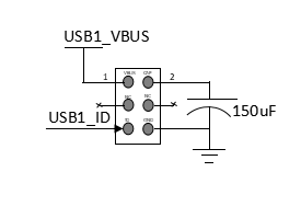
GUID-A9494F94-BA98-4CAC-A595-23E90193CAF8-low.pngFigure 3-19 J4 Header for USB2.0 Host Interface