SPRUIM6A October 2018 – November 2020
- 1Introduction
- 2AM65x IDK Overview
-
3Common Processor Board
- 3.1 Key Features
- 3.2 Functional Block Diagram
- 3.3
Overview of Common Processor Board
- 3.3.1 Clocking
- 3.3.2 Reset
- 3.3.3 Power Requirements
- 3.3.4 Configuration
- 3.3.5 Memory Interfaces
- 3.3.6 Ethernet Interface
- 3.3.7 LCD Display Interface
- 3.3.8 USB 2.0 Interface
- 3.3.9 CSI-2 Interface
- 3.3.10 Application Card Interface
- 3.3.11 SERDES Interface
- 3.3.12 GPMC/DSS Interface
- 3.3.13 I2C Interface
- 3.3.14 SPI Interface
- 3.3.15 Timer and Interrupt
- 3.3.16 Fan Connector
- 4IDK Application Card
- 5x2 Lane PCIe Personality Card
-
6Known Issues
- 6.1 Determining the Revision and Date Code for the EVM
- 6.2 Known Issues for the A, E4, and E3 Revision
- 6.3 Known Issues for the E4 & E3 Revision
- 6.4
Known Issues for the E3 Revision
- 6.4.1 Resonance Observed on the SoC Side of Some Filters Associated with VDDA_1V8
- 6.4.2 Additional LDO Power Supply Needed for VDDA_1P8_SERDES0
- 6.4.3 Length of the RESET Signal to the PCIE Connectors on the SERDES Daughter Card
- 6.4.4 The PORz_OUT and MCU_PORz_OUT Signals Go High During Power Sequencing
- 6.4.5 Orientation of the Current Monitoring Shunt Resistors
- 6.4.6 SD Card IO Supply Capacitance
- 6.4.7 PHY Resistor Strapping Changed to Disable EEE Mode
- 6.4.8 The I2C Address for the I2C Boot Memory changed to 0x52
- 7Configuring the PRG0 and PRG1 Ethernet Interface to MII
- 8Revision History
3.3.6.1 Gigabit Ethernet PHY Default Configuration
The default configuration of the DP83867 is determined using a number of resistor pull-up and pull-down values on specific pins of the PHY. Depending on the values installed, each of the configuration pins can be set to one of four modes by using the pull-up and pull-down options provided. The AM65x IDK uses the 48-pin QFN package, designated with the RGZ suffix, which only supports the RGMII interface.
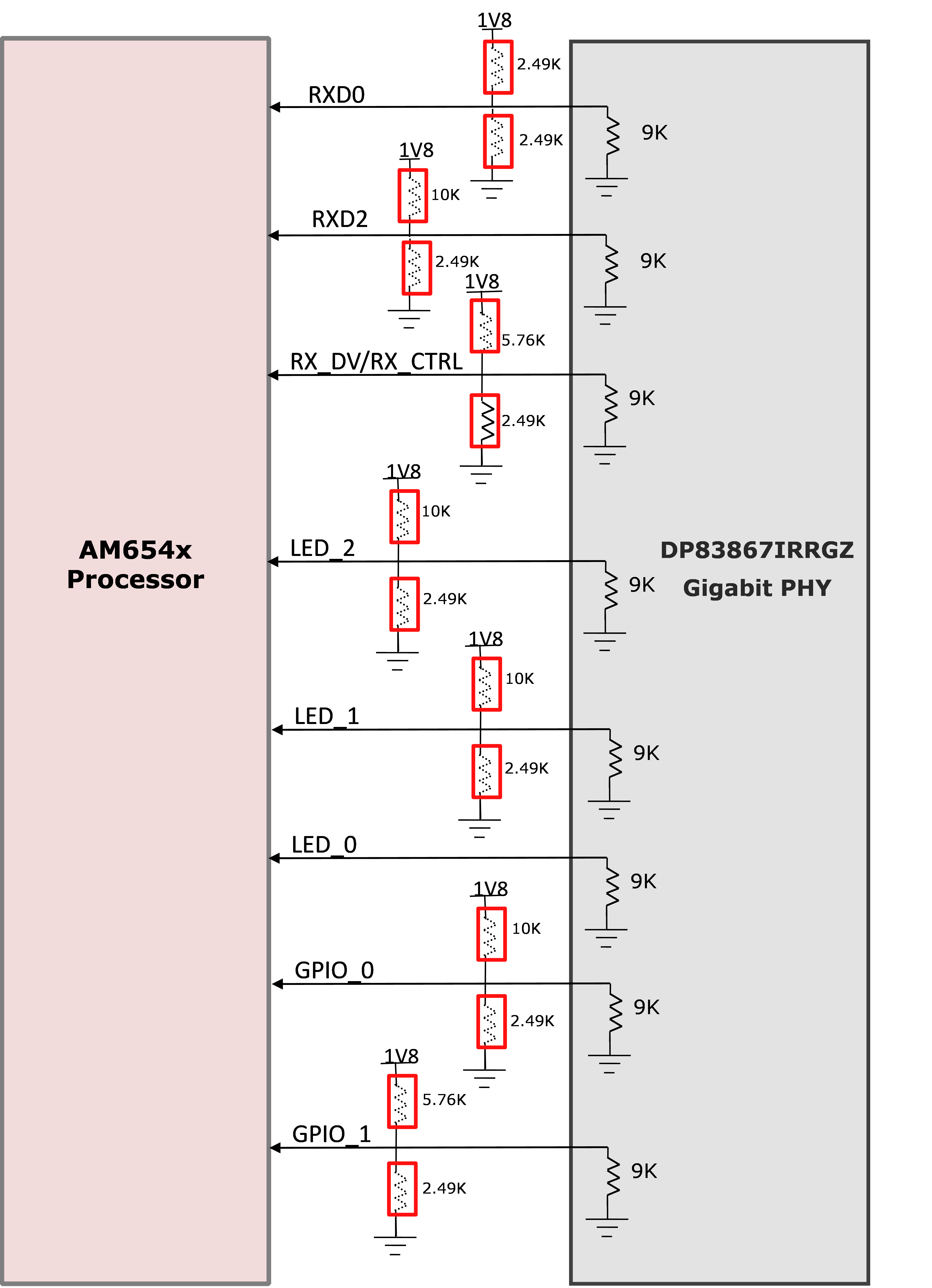
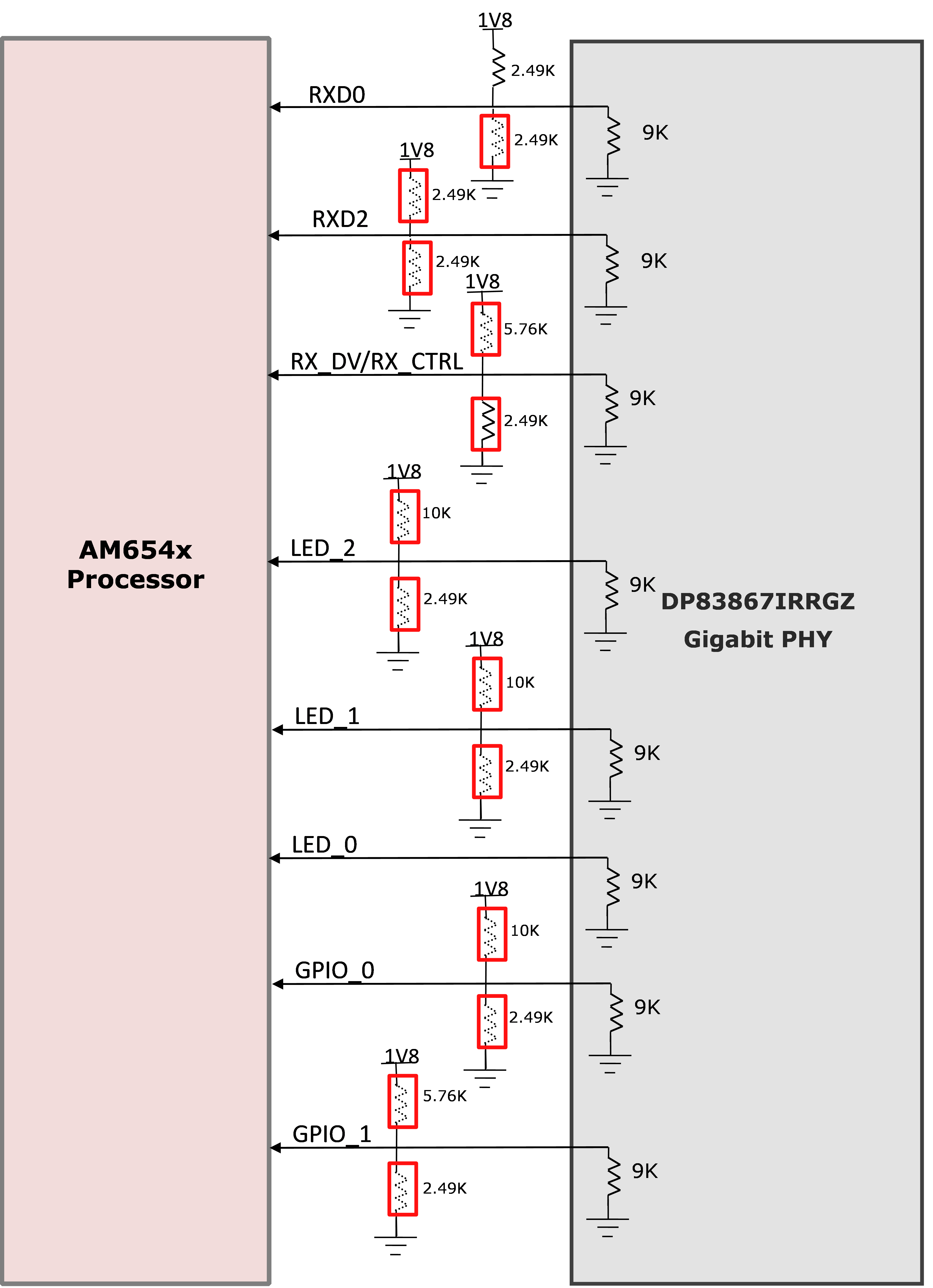
The DP83867 PHY uses four level configurations based on resistor strapping, which generate four distinct voltage ranges. The resistors are connected to the RX data and control pins, which are normally driven by the PHY and are inputs to the processor. The voltage range for each mode is shown below:
Mode 1 - 0 V to 0.1764 V
Mode 2 – 0.252 V to 0.3438 V
Mode 3 – 0.405 V to 0.5112 V
Mode 4 – 1.2492 V to 1.5984 V
Default configurations of all phys are mentioned in Table 3-23.
| Signal | Mode | Default Configuration | Configuration | Description | |||
|---|---|---|---|---|---|---|---|
| Pull Up | Pull Down | ||||||
| PRG2 RGMII1 PHY (J14A) | RX_D0 | 1 | Open | Open | PHY_AD1 = 0 and PHY_AD0 = 0 | Address of the PHY is set to 00000 | |
| RX_D2 | 1 | Open | Open | PHY_AD3 = 0 and PHY_AD2 = 0 | |||
| RX_DV/RX_CTRL | 1 | Open | Open | N/A | N/A | ||
| LED_2 | 1 | Open | Open | RGMII Clock Skew TX[1]=0 and RGMII Clock Skew TX[0]=0 | RGMII Clock Skew TX = 2 ns and advertise | ||
| LED_1 | 1 | Open | Open | ANEG_SEL=0 and RGMII Clock Skew TX[1]=0 | |||
| GPIO_0 | 1 | Open | Open | RGMII Clock Skew RX[0]=0 | RGMII Clock Skew RX = 2 ns | ||
| GPIO_1 | 1 | Open | Open | RGMII Clock Skew RX[2]=0 and RGMII Clock Skew RX[1]=0 | |||
| PRG2 RGMII1 PHY (J14B) | RX_D0 | 4 | 2.49K | Open | PHY_AD1 = 1 and PHY_AD0 = 1 | Address of the PHY is set to 00011 | |
| RX_D2 | 1 | Open | Open | PHY_AD3 = 0 and PHY_AD2 = 0 | |||
| RX_DV/RX_CTRL | 1 | Open | Open | N/A | N/A | ||
| LED_2 | 1 | Open | Open | RGMII Clock Skew TX[1]=0 and RGMII Clock Skew TX[0]=0 | RGMII Clock Skew TX = 2 ns and advertise | ||
| LED_1 | 1 | Open | Open | ANEG_SEL=0 and RGMII Clock Skew TX[1]=0 | |||
| GPIO_0 | 1 | Open | Open | RGMII Clock Skew RX[0]=0 | RGMII Clock Skew RX = 2 ns | ||
| GPIO_1 | 1 | Open | Open | RGMII Clock Skew RX[2]=0 and RGMII Clock Skew RX[1]=0 | |||
| PRG2 RGMII1 PHY (J12) | RX_D0 | 1 | Open | Open | PHY_AD1 = 0 and PHY_AD0 = 0 | Address of the PHY is set to 00000 | |
| RX_D2 | 1 | Open | Open | PHY_AD3 = 0 and AN2 = 0 | |||
| RX_DV/RX_CTRL | 1 | Open | Open | N/A | N/A | ||
| LED_2 | 1 | Open | Open | RGMII Clock Skew TX[1]=0 and RGMII Clock Skew TX[0]=0 | RGMII Clock Skew TX = 2 ns and advertise | ||
| LED_1 | 1 | Open | Open | ANEG_SEL=0 and RGMII Clock Skew TX[1]=0 | |||
| GPIO_0 | 1 | Open | Open | RGMII Clock Skew RX[0]=0 | RGMII Clock Skew RX = 2 ns | ||
| GPIO_1 | 1 | Open | Open | RGMII Clock Skew RX[2]=0 and RGMII Clock Skew RX[1]=0 | |||
 Figure 3-16 Strapping Diagram for MCU and PRG2-RGMII1 Ethernets
 Figure 3-17 Strapping Diagram for PRG2-RGMII2 Ethernet
Resistors which are highlighted in red color boxes are DNI components.