SPRUJ10D May 2022 – September 2023
- 1
- Abstract
- Trademarks
- 1Preface: Read This First
- 2Kit Overview
- 3Board Setup
-
4Hardware Description
- 5.1 Functional Block Diagram
- 5.2 GPIO Mapping
- 5.3 Reset
- 5.4 Clock
- 5.5 Memory Interface
- 5.6 Ethernet Interface
- 5.7 I2C
- 5.8 Industrial Application LEDs
- 5.9 SPI
- 5.10 UART
- 5.11 MCAN
- 5.12 FSI
- 5.13 JTAG
- 5.14 Test Automation Header
- 5.15 LIN
- 5.16 MMC
- 5.17 ADC and DAC
- 5.18 EQEP and SDFM
- 5.19 EPWM
- 5.20 BoosterPack Headers
- 5.21 Pinmux Mapping
- 5References
- 6Revision History
4.14 Test Automation Header
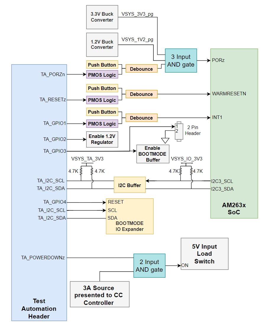
The AM263x LaunchPad supports a 40 pin test automation header that allows an external controller to manipulate basic operations such as power down, PORz, warm reset, and bootmode control.
 Figure 4-17 Test Automation Header
The Test Automation Circuit is powered by a dedicated 3.3V power supply (VSYS_TA_3V3) which is generated by a 5V to 3.3V buck regulator (TPS62177DQCR).
The AM263x SoC I2C3 instance is connected to both the Test Automation Header and the bootmode IO expander (TCA6408ARGTR).
The following table details the Test Automation GPIO mapping:
Table 4-12 Test Automation GPIO Mapping
| Signal Name | Description | Direction |
|---|---|---|
| TA_POWERDOWN | when logic low, disables the 3.3V buck regulator (TPS62913RPUR) that is used in the first stage of DC/DC conversion | Output |
| TA_PORZn | when logic low, connects the PORz signal to ground due to the PMOS V_GS being less than zero creating a power on reset to the MAIN domain | Output |
| TA_RESETz | when logic low, connects the WARMRESETn signal to ground due to the PMOS V_GS being less than zero creating a warm reset to the MAIN domain | Output |
| TA_GPIO1 | when logic low, connects the INTn signal to ground due to the PMOS V_GS being less than zero creating an interrupt to the SoC | Output |
| TA_GPIO2 | when logic low, disables the 1.2V buck regulator (TPS62913RPUR) | Output |
| TA_GPIO3 | when logic low, disables the bootmode buffer output enable | Output |
| TA_GPIO4 | Reset signal for Bootmode IO Expander (TCA6408ARGTR) | Output |