SPRUJ10D May 2022 – September 2023
- 1
- Abstract
- Trademarks
- 1Preface: Read This First
- 2Kit Overview
- 3Board Setup
-
4Hardware Description
- 5.1 Functional Block Diagram
- 5.2 GPIO Mapping
- 5.3 Reset
- 5.4 Clock
- 5.5 Memory Interface
- 5.6 Ethernet Interface
- 5.7 I2C
- 5.8 Industrial Application LEDs
- 5.9 SPI
- 5.10 UART
- 5.11 MCAN
- 5.12 FSI
- 5.13 JTAG
- 5.14 Test Automation Header
- 5.15 LIN
- 5.16 MMC
- 5.17 ADC and DAC
- 5.18 EQEP and SDFM
- 5.19 EPWM
- 5.20 BoosterPack Headers
- 5.21 Pinmux Mapping
- 5References
- 6Revision History
4.20 BoosterPack Headers
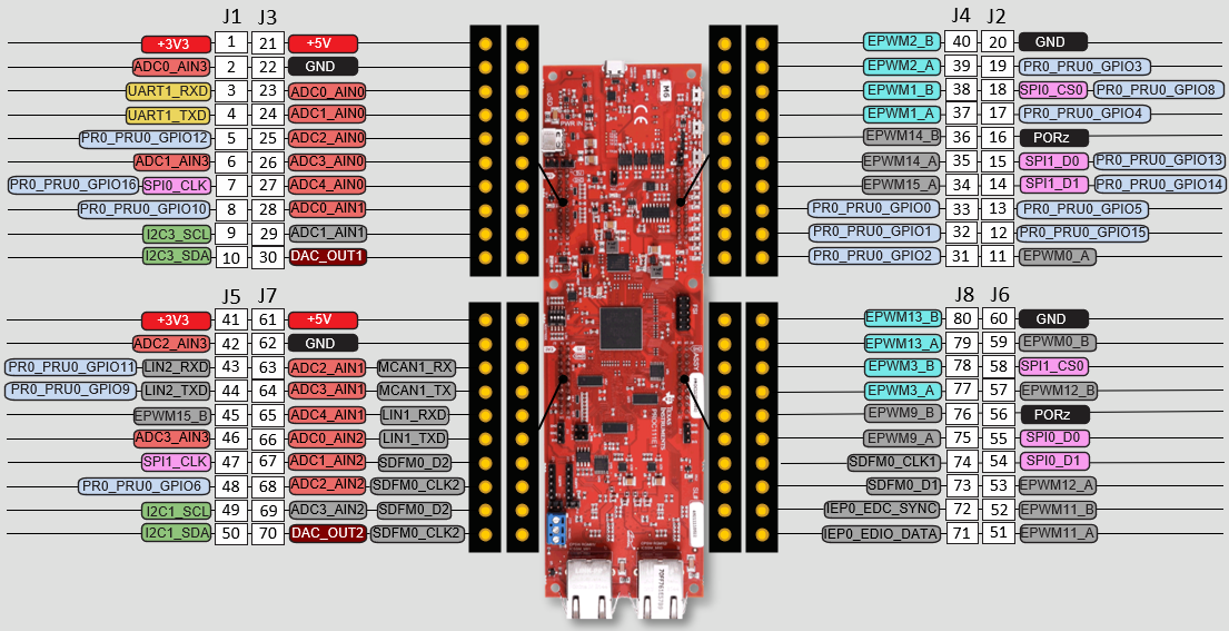
 Figure 4-24 AM263x LaunchPad BoosterPack Pinout
Note: This pinout represents the default signals mapped to the BoosterPack Header.
Additional signal options for each header are available through Pinmuxing. Two signals for one pin represents an externally
muxed option
Note: A gray background for a signal on the pinout shows that the signal does not follow
the BoosterPack Standard pinout.
The AM263x LaunchPad supports two fully independent BoosterPack XL connectors. BoosterPack site #1 (J1/J3, J2/J4) is located in between the SoC and the micro-B USB Connector. BoosterPack site #2 (J5/J7, J6/J8) is located in between the SoC and the RJ45 connectors. Each GPIO has multiple functions available through the GPIO mux. The signals connected from the SoC to the BoosterPack headers include:
- Various ADC inputs
- DAC Out
- UART1
- Various GPIO signals
- SPI0 and SPI1
- I2C1 and I2C3
- Various EPWM Channels
- LIN1 and LIN2
- MCAN1
- SDFM0