SPRUJ63A September 2022 – October 2023
- 1
- Trademarks
- 1Introduction
- 2Important Usage Notes
-
3System Description
- 3.1 Key Features
- 3.2 Functional Block Diagram
- 3.3 Power-On/Off Procedures
- 3.4
Peripheral and Major Component
Description
- 3.4.1 Clocking
- 3.4.2 Reset
- 3.4.3 Power
- 3.4.4 Configuration
- 3.4.5 JTAG
- 3.4.6 Test Automation
- 3.4.7 UART Interfaces
- 3.4.8 Memory Interfaces
- 3.4.9 Ethernet Interface
- 3.4.10 Display Interface
- 3.4.11 USB 2.0 Interface
- 3.4.12 PCIe Interface
- 3.4.13 High Speed Expansion Interface
- 3.4.14 CAN Interface
- 3.4.15 Interrupt
- 3.4.16 ADC Interface
- 3.4.17 Safety Connector
- 3.4.18 SPI Interfaces
- 3.4.19 I2C Interfaces
- 3.4.20 FSI Interface
- 4Known Issues and Modifications
- 5References
- 6Revision History
3.4.20 FSI Interface
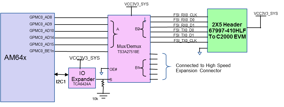
One FSI Interface (1Tx and 1Rx) from SoC is terminated on the 2x5 header with part number 67997-410HLF from Amphenol ICC (FCI) having connections, which can be interfaced to C2000 EVM. FSI_TX0 signals and FSI_RX0 signals are connected to the mux so that the signals are available to both the FSI connector and the expansion connector. The TS3A27518E mux-demux is used for this purpose and is controlled by GPIO from IO Expander. A logic low in Mux select pin connects port A and Port B1, whereas a logic high connects A port to B2 port. The default state of mux drives the signals from A port to B1 port, which is connected to HSE connector.
| Pin No. | Signal |
|---|---|
| 1 | FSI_TX0_CLK |
| 2 | FSI_RX0_CLK |
| 3 | DGND |
| 4 | DGND |
| 5 | FSI_TX0_D0 |
| 6 | FSI_RX0_D0 |
| 7 | FSI_TX0_D1 |
| 8 | FSI_RX0_D1 |
| 9 | DGND |
| 10 | VCC_3V3_SYS |
 Figure 3-31 AM64x/AM243x FSI Interface