SPRUJ63A September 2022 – October 2023
- 1
- Trademarks
- 1Introduction
- 2Important Usage Notes
-
3System Description
- 3.1 Key Features
- 3.2 Functional Block Diagram
- 3.3 Power-On/Off Procedures
- 3.4
Peripheral and Major Component
Description
- 3.4.1 Clocking
- 3.4.2 Reset
- 3.4.3 Power
- 3.4.4 Configuration
- 3.4.5 JTAG
- 3.4.6 Test Automation
- 3.4.7 UART Interfaces
- 3.4.8 Memory Interfaces
- 3.4.9 Ethernet Interface
- 3.4.10 Display Interface
- 3.4.11 USB 2.0 Interface
- 3.4.12 PCIe Interface
- 3.4.13 High Speed Expansion Interface
- 3.4.14 CAN Interface
- 3.4.15 Interrupt
- 3.4.16 ADC Interface
- 3.4.17 Safety Connector
- 3.4.18 SPI Interfaces
- 3.4.19 I2C Interfaces
- 3.4.20 FSI Interface
- 4Known Issues and Modifications
- 5References
- 6Revision History
3.4.1.1 Ethernet PHY Clock
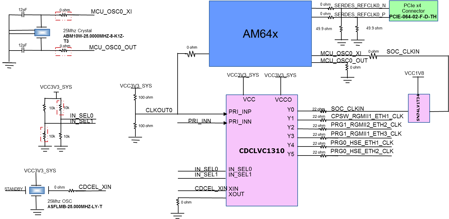
A clock generator of part number CDCLVC1310 is used to drive 25 MHz clock to the Ethernet PHYs. CDCLVC1310 is a 1:10 LVCMOS clock buffer, which takes 25 MHz crystal/LVCMOS reference input and provides ten 25 MHz LVCMOS clock outputs. The source for the clock buffer is either the CLKOUT0 pin from the SoC or a 25 MHz oscillator (ASFLMB-25.000MHZ-LY-T), the selection is made using a set of resistors. This selection can be made through the select lines of the clock buffer.
- IN_SEL0, IN_SEL1 = [00] for selecting CLKOUT0.
- IN_SEL0, IN_SEL1 = [01] for selecting oscillator input. This is the default condition.
The resistor termination for single ended Crystal input is provided as per device-specific data sheet.
| IN_SEL1 | IN_SEL0 | Clock Chosen | Mount | Unmount |
|---|---|---|---|---|
| 0 | 0 | EXT_REFCLK from SoC | R40, R45 | R248, R253 |
| 1 | 0 | Oscillator input | R253, R40 | R45, R248 |
 Figure 3-4 AM64x/AM243x EVM Clock Tree