SSZT196 february 2021 OPA2333 , OPA391 , TLV8802 , TLV9002 , TLV9042
In recent years, the popularity of battery-powered electronics has made power consumption an increasing priority for analog circuit designers. With this in mind, this article is the first in a series that will cover the ins and outs of designing systems with low-power operational amplifiers (op amps).
In the first installment, I will discuss power-saving techniques for op-amp circuits, including picking an amplifier with a low quiescent current (IQ) and increasing the load resistance of the feedback network.
Understanding power consumption in op-amp circuits
Let’s begin by considering an example circuit where power may be a concern: a battery-powered sensor generating an analog, sinusoidal signal of 50 mV amplitude and 50 mV of offset at 1 kHz. The signal needs to be scaled up to a range of 0 V to 3 V for signal conditioning (Figure 1), while saving as much battery power as possible, and that will require a noninverting amplifier configuration with a gain of 30 V/V, as shown in Figure 2. How can you optimize the power consumption of this circuit?
 Figure 1 Input and output
signals
Figure 1 Input and output
signals Figure 2 A sensor amplification circuit
Power consumption in an op-amp circuit consists of various factors: quiescent power, op amp output power, and load power. The quiescent power, PQuiescent, is the power needed to keep the amplifier turned on and consists of the op amp’s IQ, which is listed in the product data sheet. The output power, POutput, is the power dissipated in the op amp’s output stage to drive the load. Finally, load power, PLoad, is the power dissipated by the load itself. My colleague, Thomas Kuehl, in his technical article, “Top questions on op-amp power dissipation – part 1,” and a TI Precision Labs video, “Op Amps: Power and Temperature,” define various equations for calculating power consumption for an op amp circuit.
In this example, we have a single-supply op amp with a sinusoidal output signal that has a DC voltage offset. So we will use the following equations to find the total, average power, Ptotal,avg. The supply voltage is represented by V+. Voff is the DC offset of the output signal and Vamp is the output signal’s amplitude. Finally, RLoad is the total load resistance of the op amp. Notice that the average total power is directly related to IQ while inversely related to RLoad.
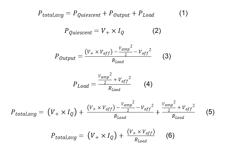
Picking a device with the right IQ
Equations 5 and 6 have several terms and it’s best to consider them one at a time. Selecting an amplifier with a low IQ is the most straightforward strategy to lower the overall power consumption. There are, of course, some trade-offs in this process. For example, devices with a lower IQ typically have lower bandwidth, greater noise and may be more difficult to stabilize. Subsequent installments of this series will address these topics in greater detail.
Because the IQ of op amps can vary by orders of magnitude, it’s worth taking the time to pick the right amplifier. TI offers circuit designers a broad selection range, as you can see in Table 1. For example, the TLV9042, OPA2333, OPA391 and other micropower devices deliver a good balance of power savings and other performance parameters. For applications that require the maximum power efficiency, the TLV8802 and other nanopower devices will be a good fit. You can search for devices with your specific parameters, such as those with ≤10 µA of IQ, using our parametric search.
| Typical specifications | TLV9042 | OPA2333 | OPA391 | TLV8802 |
|---|---|---|---|---|
| Supply voltage (VS) | 1.2 V-5.5 V | 1.8 V-5.5 V | 1.7 V-5.5 V | 1.7 V-5.5 V |
| Bandwidth (GBW) | 350 kHz | 350 kHz | 1 MHz | 6 kHz |
| Typical IQ per channel at 25°C | 10 µA | 17 µA | 22 µA | 320 nA |
| Maximum IQ per channel at 25°C | 13 µA | 25 µA | 28 µA | 650 nA |
| Typical offset voltage (Vos) at 25°C | 600 µV | 2 µV | 10 µV | 550 µV |
| Input voltage noise density at 1 kHz (en) | 66 nV/√Hz | 55 nV/√Hz | 55 nV/√Hz | 450 nV/√Hz |
Reducing the resistance of the load network
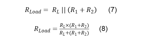
Now consider the rest of the terms in Equations 5 and 6. The Vamp terms cancel out with no effect on Ptotal,avg and Voff is generally predetermined by the application. In other words, you often cannot use Voff to lower power consumption. Similarly, the V+ rail voltage is typically set by the supply voltages available in the circuit. It may appear that the term RLoad is also predetermined by the application. However, this term includes any component that loads the output and not just the load resistor, RL. In the case of the circuit shown in Figure 1, RLoad would include RL and the feedback components, R1 and R2. Hence, RLoad would be defined by Equations 7 and 8.
By increasing the values of the feedback resistors, you can decrease the output power of the amplifier. This technique is especially effective when Poutput dominates PQuiescent, but has its limits. If the feedback resistors become significantly larger than RL, then RL will dominate RLoad such that the power consumption will cease to shrink. Large feedback resistors can also interact with the input capacitance of the amplifier to destabilize the circuit and generate significant noise.
To minimize the noise contribution of these components, it’s a good idea to compare the thermal noise of the equivalent resistance seen at each of the op-amp’s inputs (see Figure 3) to the amplifier’s voltage noise spectral density. A rule of thumb is to ensure that the amplifier’s input voltage noise density specification is at least three times greater than the voltage noise of the equivalent resistance as viewed from each of the amplifier’s inputs.
 Figure 3 Resistor thermal noise
Real-world example
Using these low-power design techniques, let’s return to the original problem: a battery-powered sensor generating an analog signal of 0 to 100 mV at 1 kHz needs a signal amplification of 30 V/V. Figure 4 compares two designs. The design on the left uses a typical 3.3-V supply, resistors not sized with power-savings in mind and the TLV9002 general-purpose op amp. The design on the right uses larger resistor values and the lower-power TLV9042 op amp. Notice that the noise spectral density of the equivalent resistance, approximately 9.667 kΩ, at the TLV9042’s inverting input is more than three times smaller than the broadband noise of the amplifier in order to ensure that the noise of the op amp dominates any noise generated by the resistors.
 Figure 4 A typical design vs. a
power-conscious design
Figure 4 A typical design vs. a
power-conscious designUsing the values from Figure 4, the design specifications and the applicable amplifier specifications, Equation 6 can be solved to give Ptotal,avg for the TLV9002 design and the TLV9042 design. For your reading convenience, Equation 6 has been copied here as Equation 9. Equations 10 and 11 show the numeric values of Ptotal,avg for the TLV9002 design and the TLV9042 design, respectively. Equations 12 and 13 show the results.
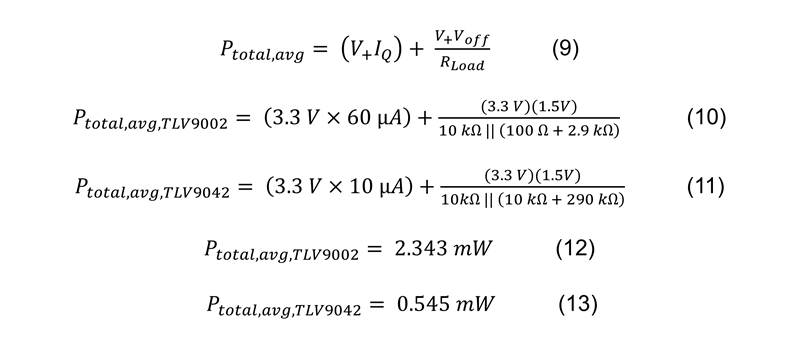
As can be seen from the last two equations, the TLV9002 design consumes more than four times the power of the TLV9042 design. This is a consequence of a higher amplifier IQ, demonstrated in the left terms of Equations 10 and 11, along with smaller feedback resistors, as accounted for in the right terms of Equations 10 and 11. In the case where more IQ and smaller feedback resistors are not needed, implementing the techniques described here can provide significant power savings.
Conclusion
I’ve covered the basics of designing amplifier circuits for low power consumption, including picking a device with low IQ and increasing the values of the discrete resistors. In part 2 of this series, I’ll take a look at when you can use low-power amplifiers with low voltage supply capabilities.
Additional resources
- Catch up on other installments in the “Designing with low-power op amps” series.
- Keep reading with the next installment in this series, "Designing with low-power op amps, part 2: Low-power op amps for low-supply-voltage applications."
- Learn how to work with op amps in TI Precision Labs - Op amps, a series of on-demand tutorials covering basic to advanced topics.