SSZT285 july 2020 BQ25790 , BQ25798
The buck-boost charger has become increasingly popular in recent years given its ability to charge a battery from nearly any input source, regardless of whether the input voltage is higher or lower than the battery voltage.
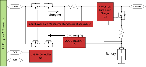
One critical benefit of the widespread adoption of USB Type-C is a realistic path to a universal adapter and corresponding e-waste reduction. Although the USB Type-C connector is unified, adapter power ratings and voltages still have large variations, including the legacy 5-V USB adapter and USB PD adapters capable of providing a voltage range from 5 V to 20 V. In addition, different portable devices might have different numbers of cell batteries inside. These variabilities in input voltage and battery voltage require a buck-boost topology for battery-charger integrated circuits (ICs). The high power density buck-boost chargers should not only integrate the general charging functional blocks, but also integrate the additional components in the USB PD charging system, such as load switches and DC/DC converters, to streamline system design, reduce bill-of-materials (BOM) cost and keep the overall solution size small. Figure 1 shows a system block diagram for a USB PD charging solution.
 Figure 1 Block diagram for a USB PD
charging solution.
Figure 1 Block diagram for a USB PD
charging solution.In order to support the USB On-the-Go (OTG) specification, one DC/DC converter discharges the battery to build up a regulated voltage at VBUS and power external devices when the adapter is not present. If the USB Type-C port requires fast role swap (FRS), the DC/DC converter has to be enabled and kept on standby all the time, even if an adapter is plugged into the USB Type-C port. When the adapter is disconnected, the back-to-back MOSFETs in the discharging power path turn on, passing the U3 output voltage to VBUS and holding on the VBUS voltage. Keeping the DC/DC converter always on actually causes extra quiescent current loss for the entire system.
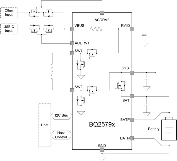
The fully integrated buck-boost charger shown in Figure 2 can simplify the system-level design of a USB PD charging solution. First, the input current sensing is integrated into the charge. With this sensed input current, the charger provides the input current regulation and input overcurrent protection to avoid adapter overload. As part of the input overvoltage and overcurrent protection circuit, the control logic and driving circuitry for the external back-to-back MOSFETs are also integrated into the charger. These features make it possible to eliminate the unit that supports input power-path management and input current sensing from the block diagram.
Implementing the bidirectional operation of the four FETs’ buck-boost converter allows the charger to support OTG mode itself. When the adapter is present, the charger operates in forward charging mode with power flow from VBUS to the battery. When the adapter is disconnected, the power flow reverses from the battery to VBUS. The OTG mode output voltage at VBUS covers the full USB PD voltage range, from 2.8 V to 22 V with a 10-mV programmable step size, which is compatible with the USB PD 3.0 specification.
 Figure 2 The proposed fully integrated
buck-boost charger.
Figure 2 The proposed fully integrated
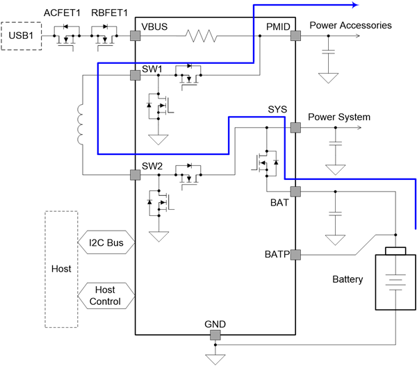
buck-boost charger.In order to support FRS for the USB Type-C port, this integrated buck-boost charger implements a novel backup mode. In this context, backup mode refers to an ultra-fast transition for the buck-boost charger from forward charging mode to reverse OTG mode without the bus voltage crashing. Looking at the application diagram in Figure 3, the adapter connects at the USB port, powering the system and charging the battery through the buck-boost power stage. At the same time, the adapter could power accessories from the charger’s PMID output. When the adapter is disconnected, the battery’s internal FET can still power the system; however, the accessories at PMID might lose power.
With backup mode enabled, the charger is able to monitor the VBUS voltage; the VBUS voltage dropping lower than the preset threshold indicates the adapter’s removal. Once it detects a removal, the charger shifts from forward charging mode to OTG mode with minimal delay time, discharges the battery to regulate the VBUS voltage, and achieves FRS by itself. When the adapter is unplugged, the sources to power the system and accessories can switch from the adapter to the battery seamlessly, making it possible to eliminate the DC/DC converter for OTG mode and FRS from the block diagram.
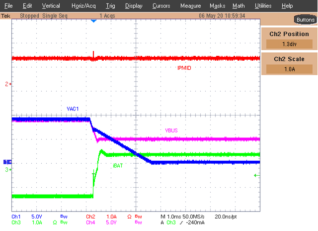
Figure 4 shows the tested waveforms of the charger backup mode for FRS. A 9-V adapter is connected at USB1 as the input power. VBUS is shorted to the adapter by turning on ACFET1-RBFET1. Assume that there is a 1-A accessory current at PMID and a 1-A charging current at BAT. When the 9-V adapter voltage (VAC) is gone, the PMID and VBUS can still be regulated at 5 V to continuously power the 1-A PMID load.
 Figure 3 USB Type-C FRS realized by
single buck-boost charger.
 Figure 4 Buck-boost charger FRS from
VBUS sink to VBUS source.
Figure 4 Buck-boost charger FRS from
VBUS sink to VBUS source.All of the features described above help simplify the system-level design of a USB PD charging solution, and TI has implemented in our latest buck-boost chargers, the BQ25790 and BQ25798. These chargers support one cell in series (1s) to 4s battery charging from a 3.6-V to 24-V input voltage, covering the full USB PD input voltage range.
These features are available in a 2.9-mm-by-3.3-mm wafer chip-scale package or a 4-mm-by-4-mm quad flat no-lead package. The total charging solution is capable of delivering 45 W of power, with around 100 W/in2 (150mV/mm2) of power density, which two times more than competitive devices.
Additional resources
- Read the BQ25790 data sheet and the BQ25798 data sheet.
- Read the technical article, Universal and fast charging – a future trend for battery-powered applications.
- Read the technical article, Transform the way you charge your devices with USB Type-C and PD.