SSZT298 june 2020 LM25180 , LM25180-Q1 , LM25183 , LM25183-Q1 , LM25184 , LM25184-Q1 , LM5180 , LM5180-Q1 , LM5181 , LM5181-Q1
For low-power isolated designs that require an extended product life cycle, such as gate-driver bias for automotive traction inverters, or 4- to 20-mA loop sensors in field transmitters for factory automation applications, many designers choose to leverage the reliability and simplicity of a primary-side regulated (PSR) multioutput flyback converter. Two key attributes of the PSR flyback are:
- Reliability and ease of use, with only one component – the power transformer – crossing the isolation barrier. Feedback regulation does not require an optocoupler, auxiliary winding, signal transformer or external reference.
- Low total component count, especially when multiple isolated outputs are required.
In this technical article, I’ll review a stacked-output PSR flyback design that optimizes regulation performance.
Stacked isolated outputs
It is possible to easily design a PSR flyback converter for multiple outputs with flexible secondary-side configurations; for example, with bipolar outputs (such as ±12 V or 15 V/-8 V) or dual-positive outputs (such as 3.3 V/12 V or 5 V/15 V) that share a common ground, or as independent outputs with different ground references.
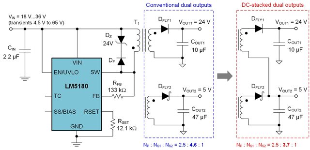
In this context, take a look at the PSR flyback converter circuit in Figure 1 using the LM5180. The secondary-side circuit on the left (enveloped in blue) delivers dual outputs of 24 V and 5 V, designated as VOUT1 and VOUT2, respectively. Meanwhile, the secondary-side circuit on the right (surrounded in red) shows an equivalent implementation with DC-stacked outputs by referencing an upper secondary winding that provides 19 V on top of a 5-V output. Note the transformer turns ratios indicated for each design.
 Figure 1 PSR flyback converter schematic with dual outputs, using conventional and DC-stacked winding arrangements
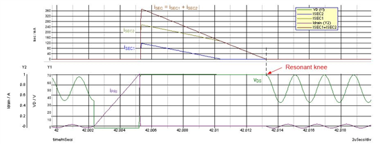
Appropriately timed sensing of the switch voltage at its resonant knee position provides a suitable proxy of the output voltage to achieve very tight regulation accuracy across line, load and temperature ranges. However, the demagnetization time is not uniquely defined with multiple outputs. Each winding has its own demagnetization interval, with the voltage sampled at the end of the last demagnetization. In the simulated waveforms shown in Figure 2, the normalized secondary currents add up to the expected triangular magnetizing current waveform.
 Figure 2 Switch-node voltage and winding current waveforms in a dual-output PSR flyback converter, where the secondary winding with the largest conduction time (SEC2) dictates regulation
The stacked winding has fewer turns and thus lower leakage inductance, and the secondary-to-secondary coupling (vital for optimized cross regulation) is tighter. Also lower is the flyback diode reverse voltage swing, which helps reduce common-mode electromagnetic interference and alleviates the capacitive current spike reflected to the primary during switch turnon.
Transformer design
With leakage inductance the major cause of poor cross-regulation in flyback circuits, here are the steps to minimize it (both primary-to-secondary and secondary-to-secondary):
- Interleave the primary winding (or, more specifically, the winding with the highest number of turns).
- Wind full layers for the best layer-to-layer coupling and fill each layer using multistrands.
- Select a core shape with wide bobbin width to achieve a minimum number of layers.
- Reduce secondary-to-secondary leakage inductance by:
- Winding secondaries bifilar or multifilar on the same layer.
- Sandwiching (shielding) low-current secondary windings between layers of high-current secondaries.
Figure 3 shows a transformer construction diagram for the design in Figure 1. The primary winding is a 50/50 series split and the secondaries are wound bifilar.
 Figure 3 Stacked-output transformer winding strategy (a); construction diagram (b)
This quick-start calculator helps streamline the selection and optimization of transformer turns ratios, magnetizing inductance and winding resistance parameters.
PCB layout
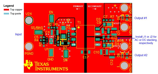
Figure 4 shows the printed circuit board (PCB) layout for a stacked output similar to that in Figure 1. This design uses the LM25184 flyback converter for higher current capability and a 13-mm-by-11-mm transformer. Jumper options configure the outputs either as DC or AC stacked, or galvanically separated as independent outputs.
 Figure 4 PCB layout of a stacked-output flyback converter
Summary
Amid a continual focus on tight regulation and high reliability, a PSR flyback converter fits a diverse set of power circuits for single- and multioutput isolated applications. The LM5180 and LM25184 are members of a PSR flyback converter family that enable high regulation accuracy in applications with power levels from 1 W to 15 W.
Additional resources
- Review the application note, “PSR Flyback DC/DC Converter Transformer Design for mHEV Applications.”
- Read the Analog Design Journal article, “Why use PSR-flyback isolated converters in dual-battery mHEV systems” and watch the related video.
- Peruse these multioutput PSR flyback reference designs:
- “4.5-V to 65-V input, compact bias supply with power stage reference design for IGBT/SiC gate drivers.”
- “Compact, efficient, 24-V input auxiliary power supply reference design for servo drives.”
- Watch this video on how to improve the cross-regulation of multioutput flybacks.