SSZT422 august 2019 ADC12DJ3200
[[This article is the second installment of a series that explains how to use scattering parameters, also known as S-parameters, in the design of direct radio-frequency (RF) sampling architectures. The first installment is here.]]
Vector Network analyzer must produce incident waves across a wide range of frequencies and amplitudes while separating and measuring the incident and reflected waves across a number of test ports. It is important to know the incident and reflected waves at a specific location for each device under test (DUT) port, hence it further increases complexity.
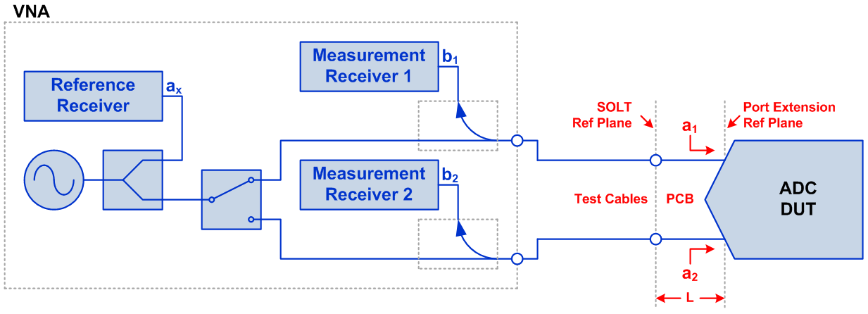
Figure 1 is a simplified block diagram of a two-port VNA. The VNA stimulates the active incident port with a tunable oscillator, which is multiplexed between the two ports with a terminating microwave switch (the unused port is connected to 50Ω). The oscillator simultaneously drives both the DUT and a reference receiver (through a power divider) to enable incident wave power measurements.
 Figure 1 Simplified Two-port VNA Block
Diagram
Figure 1 Simplified Two-port VNA Block
DiagramA directional coupler on each port separates reflected waves from incident waves, in which reflected waves are fed to three measurement receivers. All three receivers are synchronized in such a way that the relative phase of the wave quantities can be measured directly.
A measurement is made by sweeping the oscillator between the desired start and stop frequencies while capturing each of the receiver’s amplitudes and phases, with one port active at a time.
As we mentioned earlier, it’s important to measure incident and reflected waves at a specific location at each DUT port. This location is known as the reference plane and is critical to successful measurement. The process of setting the reference plane and minimizing error terms is called calibration.
The VNA has one glaring limitation when it comes to measuring analog-to-digital converters (ADCs): it does not speak digital. Since the output data stream of the ADC is numeric, combining the measurements of the VNA with the ADC’s captured data to compute the S-parameters crossing the analog to the digital domain requires an ad hoc method.
Let’s take a look at what an S-parameter test fixture looks like and how to divide and conquer the measurements required constructing a model.
| Designing for demanding requirements? | |

|
Meet the requirements of tomorrow's test and measurement applications with the fastest-ever ADC. |
The Anatomy of an ADC S-parameter Test Fixture
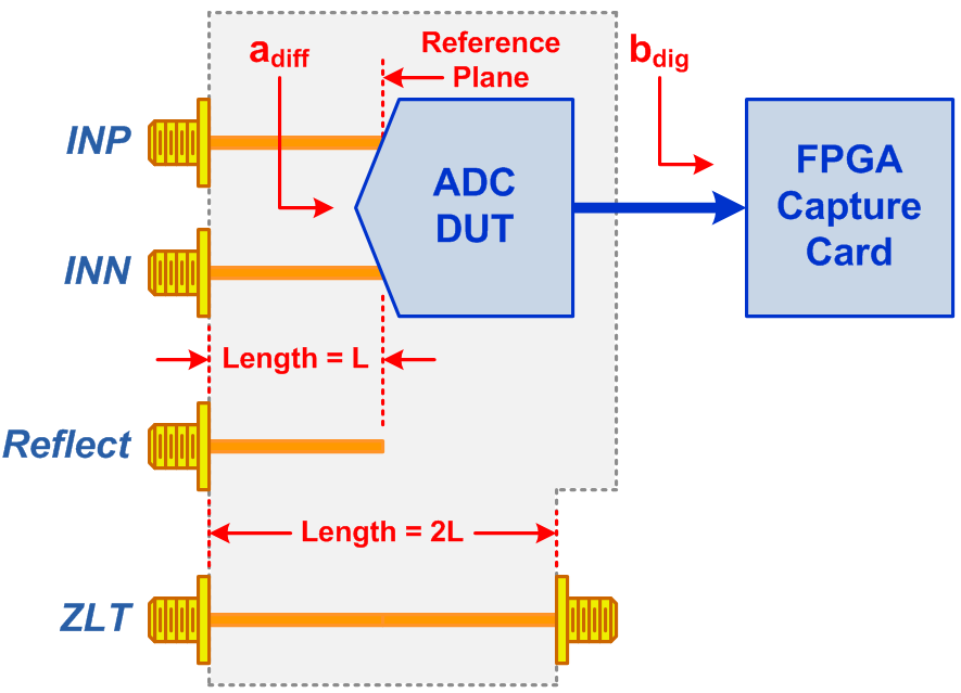
Figure 2 shows the S-parameter test fixture to measure the ADC with the VNA, including the differential coaxial input to the ADC, a high-speed data connection to the field-programmable gate array (FPGA), capture card and coaxial calibration structures.
Measuring the input impedance characteristics requires a different calibration and measurement methodology compared to that of the frequency response. Ultimately we need both measurements to construct an S-parameter model, but let’s begin with input impedance.
 Figure 2 Simplified ADC S-parameter
Test Fixture
Figure 2 Simplified ADC S-parameter
Test FixtureCalibrating the VNA for input impedance measurements is a two-step process
- Use precision short, open, load and through (SOLT) standards to move the reference plane to the end of the coaxial test cables.
- Compensate for the electrical length and loss of the test fixture connectors and transmission line interconnects.
We used the automatic port extension capability of the VNA, which uses a reflect structure on the test fixture to move the calibration plane to the DUT’s input terminals. This structure is an unterminated piece of transmission line that’s the same length as the ADC’s input interconnects. Note that while port extension is an approximation, alternative methods proved too complex to justify the small improvement in accuracy.
Measuring the ADC’s Differential Input Impedance
For this article, we measured TI’s High Speed ADC device ADC12DJ3200, which operates up to 3.2 GSPS in dual-channel mode or 6.4 GSPS in single-channel mode and has an input bandwidth of approximately 8 GHz. Figure 3 shows the VNA setup used to measure the input impedance.
A Rohde and Schwarz ZVA24 VNA was used for the device measurements. This instrument supports single-ended and differential measurements (known as true differential) where the VNA stimulates two ports simultaneously with a balanced signal. Because the ADC input is passive without feedback, measured the single-ended input impedance of each port.
 Figure 3 ADC Input Impedance
Measurement Setup
Figure 3 ADC Input Impedance
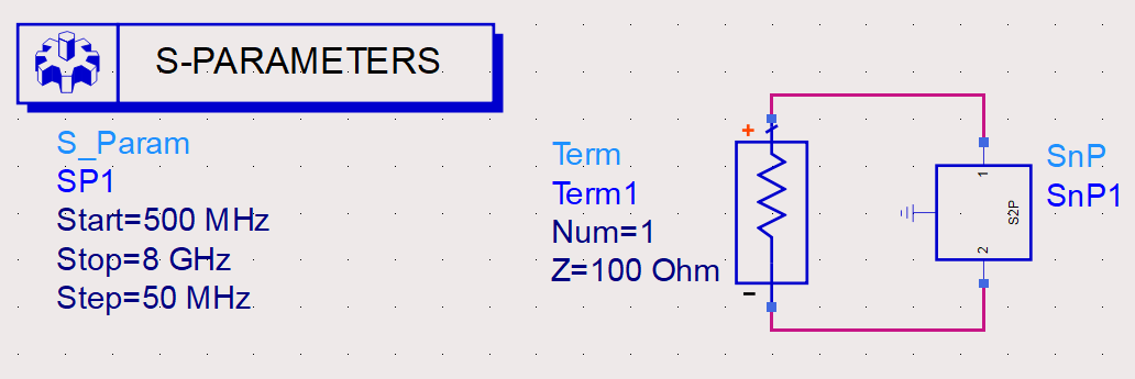
Measurement SetupAfter measuring the single-ended input impedance, the results were transformed into differential mode impedance. Figure 4 show the setup in Keysight Advanced Design System (ADS), which connects a 100 Ω port across the two single-ended ports for the simulation.
 Figure 4 Simulation Setup for
Differential Input Impedance
Figure 4 Simulation Setup for
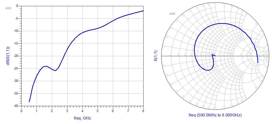
Differential Input ImpedanceFigure 5 shows the resulting impedance in both log magnitude and Smith chart formats.
 Figure 5 Differential Input Impedance
Simulation Results
Figure 5 Differential Input Impedance
Simulation ResultsSo what do these plots mean? Log magnitude (also known as the return loss when multiplied by -1) is simply 10∙log10(S11) and indicates how closely the impedance matches Z0. Return loss > 20 dB is generally considered good enough while > 10 dB is acceptable. For return loss less than 10 dB, it is necessary to perform matching for narrow band systems or add attenuation for broadband systems to prevent significant ripple caused by standing waves.
The Smith chart maps the complex impedance into a polar format. The use of a Smith chart is an entire topic itself, but here are a few pointers. The top half of the chart indicates inductive impedance and bottom half indicates capacitive impedance. The line through the center of the plot has no reactive component, which indicates a purely resistive impedance. The center point of the plot indicates an impedance of Z0 (100 Ω in this case) and the distance from the center indicates the magnitude of reflection co-efficient.
For the ADC12DJ3200, observe that the return loss gradually degrades as the frequency increases and device parasitics become dominant. The Smith chart indicates that the impedance is slightly capacitive at low frequencies and as frequency increases spirals through both inductive and capacitive values.
How could the ADC change from capacitive to inductive and back to inductive? This spiral response is common when a transmission line is inserted between the reference plane and the actual load (which has a degrading match with increasing frequency). Here, the transmission line is the routing on the device substrate between the package balls and the ADC die bumps.
Figure 5 highlights how important calibration is for useful S-parameter models. We have defined the reference plane at the ADC package balls so that the model can be used to design the printed circuit board (PCB). If the reference plane had been defined at the test fixture connectors, we would have measured entirely different complex impedance vs. frequency. The resulting model would have similar return loss, but completely different complex impedance. This would have rendered the model unusable for PCB design.
Continue reading the series in the next article, So, what's the deal with frequency response?