SSZTAO6 november 2016 LMG3410R070
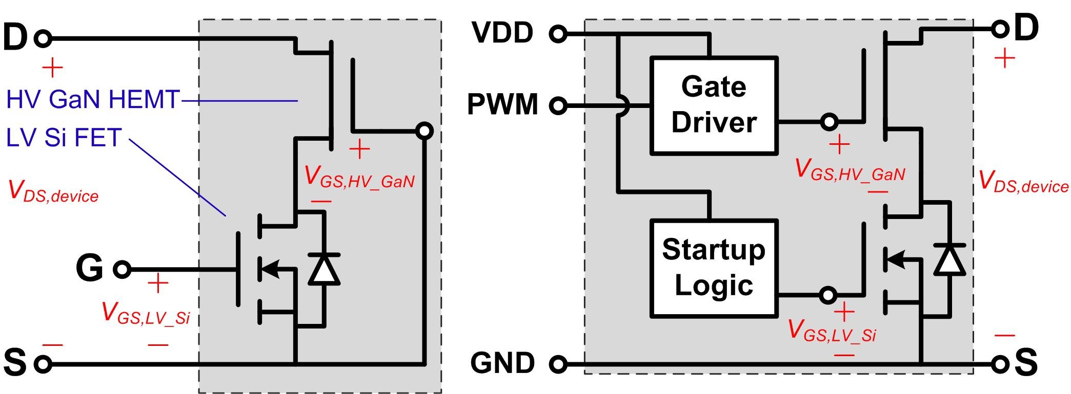
Gallium nitride (GaN) high electron mobility transistors (HEMT) improve converter efficiency, with a lower gate charge, lower output charge and lower on-resistance then silicon FETs with the same voltage rating. In high-voltage DC/DC converter applications with bus voltages greater than 380V, depletion-mode (d-mode) GaN HEMTs are more popular than enhancement-mode (e-mode) GaN HEMTs. That’s because d-mode GaN HEMTs have a much wider gate voltage range than e-mode GaN HEMTs. However, d-mode GaN HEMTs have a “normally on” feature, which is not desirable for common switch-mode power-supply applications. Two commercially available high-voltage GaN devices, shown in Figure 1, use d-mode GaN HEMTs with different configurations to form “normally off” devices.
 Figure 1 High-voltage GaN Devices Using
Synchronous Drive Technology (a); and Direct Drive Technology (b)
Figure 1 High-voltage GaN Devices Using
Synchronous Drive Technology (a); and Direct Drive Technology (b)Both GaN devices have a high-voltage GaN HEMT in series with a low-voltage silicon FET but have different driving schemes. A high-voltage GaN device with synchronous-drive technology shorts its high-voltage GaN HEMT gate pin to the source pin of its low-voltage silicon FET. By switching the low-voltage silicon FET on, you can control the on/off of the whole device.
There are three possible states of a synchronous-drive high-voltage GaN device:
- Forward blocking. When VDS,device > 0 and VGS,LV_Si < VGS(th),LV_Si, the high-voltage GaN HEMT could be either on or off, depending on whether VDS,device is higher than the high-voltage GaN HEMT VGS threshold voltage (VGS(th),HV_GaN). Notice VGS(th),LV_Si is the VGS threshold voltage of the low-voltage silicon FET. Since VGS,LV_Si < VGS(th),LV_Si, the low-voltage silicon FET is in an off state without conducting any current. If VDS,device < |VGS(th),HV_GaN|, the high-voltage GaN HEMT maintains the on state and the low-voltage silicon FET holds the VDS stress of the entire device. If VDS,device ≥ |VGS(th),HV_GaN|, the high-voltage GaN HEMT turns off and the VDS voltage of the high-voltage GaN HEMT maintains at VDS,device + VGS(th),HV_GaN, where VGS(th),HV_GaN < 0.
- Forward conduction. When VDS,device > 0 and VGS,LV_Si ≥ VGS(th),LV_Si, the low-voltage silicon FET is on. Regardless of whether the high-voltage GaN HEMT is off or on before entering the forward conduction state, the conduction of the low-voltage silicon FET will force VGS,HV_GaN ≈ 0 and turn on the high-voltage GaN HEMT.
- Reverse conduction. When VDS,device < 0 and VGS,LV_Si < VGS(th),LV_Si, VGS,HV_GaN will clamp to the low-voltage silicon FET body-diode forward voltage. Therefore, current will flow through the low-voltage silicon FET body diode and the high-voltage GaN HEMT. When VDS,device < 0 and VGS,LV_Si ≥ VGS(th),LV_Si, the low-voltage silicon FET then turns on and VGS,HV_GaN is forced to zero. Therefore, current flows through the drain-source channel of both the low-voltage silicon FET and high-voltage GaN HEMT.
Unlike synchronous-drive high-voltage GaN devices, a direct-drive high-voltage GaN device only switches the low-voltage silicon FET on once after its VDD voltage goes above undervoltage lockout. You can analyze device operation under these two conditions:
- Without VDD applied. When VDD is not yet applied to the device after applying a positive VDS,device, VGS,HV_GaN stays at a zero voltage and the VDS of the low-voltage silicon FET starts to increase. When the VDS voltage increases to VGS(th),HV_GaN, the high-voltage GaN HEMT will turn off and hold the voltage of VDS,device+VGS(th),HV_GaN. This operation is similar to the forward-blocking state of a synchronous-drive high-voltage GaN device.
- With VDD applied. After the device powers up by applying VDD, the gate driver can generate a negative voltage to turn off the high-voltage GaN HEMT directly. Once the gate driver takes control of the high-voltage GaN HEMT, the low-voltage silicon FET can then be on continuously before removing VDD or detecting any failure.
With a different driving technology, synchronous-drive high-voltage GaN devices and direct-drive high-voltage GaN devices have very different features. Synchronous-drive high-voltage GaN devices can be used as a drop-in replacement for silicon FETs. However, the low-voltage silicon FET is synchronously switched with the high-voltage GaN HEMT. That is, the body diode of the low-voltage FET may conduct current in a steady-state operation. Therefore, the low-voltage silicon FET reverse-recovery charge (Qrr) will introduce additional losses and limit the achievable switching frequency with a synchronous-drive high-voltage GaN device.
In contrast to a synchronous-drive high-voltage GaN device, the low-voltage silicon FET in a direct-drive high-voltage GaN device only switches from off to on once and stays on in steady state. This eliminates the reverse-recovery effect due to the low-voltage silicon FET body diode. In addition, the integration of gate driver and startup logic increases the reliability of whole power supply.
TI’s 600V LMG3410 GaN device adapts direct-drive technology to achieve zero Qrr and lower gate charge. Overtemperature protection (OTP) and overcurrent protection (OCP) with a 50nS fast-fault trigger time are also built in. Using TI direct-drive GaN devices in power supplies with a totem-pole switch configuration – like a totem-pole power-factor correction circuit or an inductor-inductor-capacitor (LLC) series resonant half-bridge converter – can eliminate the worry of shoot-through and improper dead-time setting.
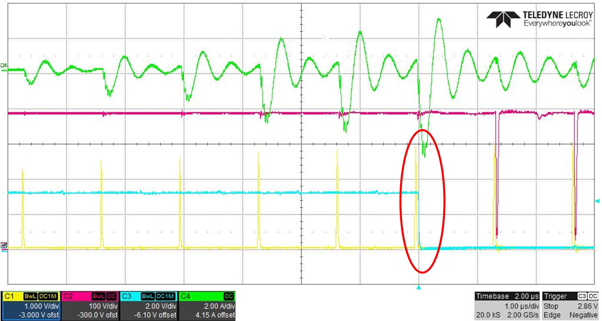
Figure 2 shows a shoot-through test on an LLC series resonant half-bridge converter with the TI LMG3410 as input switches. During the test, a high-side switch is forced on, with the low-side switch controlled by a driving signal with gradually increased duty cycles. Once the OCP trips, the LMG3410 quickly disables its driver inside to turn off the switch. This prevents the device from catastrophic failure.
We also tested LMG3410 OTP on the same LLC series resonant half-bridge board with an improper dead-time setting to force the converter into hard-switching operation.
With OCP and OTP built into this zero Qrr GaN device, you’ve cleared the most worrisome issues of totem-pole switches. Contact your local TI representative to get a LMG3410 daughtercard to evaluate how TI direct-drive GaN devices improve system reliability and efficiency.
 Figure 2 An TI LMG3410 Shoot-through
Test on an LLC Series Resonant Half-bridge Converter:
Figure 2 An TI LMG3410 Shoot-through
Test on an LLC Series Resonant Half-bridge Converter:C1 = Low-side Switch Driving Signal, C2 = Switching-node Voltage, C3 = High-side Switch Driving Signal, C4 = Primary Inductor Current
Additional Resources
- If you are interested in using TI GaN devices in your power-supply designs, see the 400V – 12V/500W High Frequency Resonant Converter Reference Design Using High Voltage GaN devices (PMP21842).
- Read the Power Supply Design Seminar paper, “GaN FET-Based CCM Totem-Pole Bridgeless PFC.”