SSZTBB2 may 2016 LP38693 , LP3878-ADJ , LP5900 , MSP430G2553 , TPL5111
Low-dropout regulators (LDOs) are widely recognized for their low noise and high power-supply rejection ratio (PSRR). However, LDOs can also contribute to power efficiency when they are complemented with the right technique. You can design a low-noise and lean power supply by pairing low-quiescent-current LDOs with appropriate power-saving techniques such as dynamic voltage scaling (DVS) or power cycling. In this blog post, I’ll present some common power-savings techniques.
DVS Methods
Mixed-signal processors such as microcontrollers (MCUs), MPUs and digital signal processors (DPSs) demand a high power supply during high-frequency processes, yet only require a fraction of that power during low-power modes or long sleep cycles. You can improve power dissipation by adjusting the voltage-supply levels accordingly to the demand. Let’s review a few popular DVS techniques and their respective technical resources.
LDO pair for dual, switchable voltage levels. The Linear Regulator Power Solution Reference Design for Reducing MSP430G2553 Power Dissipation provides test data that highlights the benefits of using two voltage levels to power MCUs like the MSP430G2553 MCU, depending on the frequency of operation. The block diagram in Figure 1 shows two LP5900 low-noise LDOs controlled by a digital signal from a host processor. The digital signal enables one LDO at a time, which means that the 3.3V LDO is enabled when the MCU needs to operate at a higher frequencies (>1MHz); the 1.8V output is enabled and the 3.3V LDO is disabled during low-frequency (<1MHz) operations. The reference design also mentions that if only one EN signal is available, you could implement a “NOT” Boolean logic gate at one of the LDO EN pins, enabling one LDO at a time.
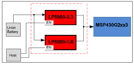 Figure 1 Linear Regulator Power Solution Reference Design Block Diagram
The pink trace in Figure 2 shows the smooth transition from a 3.3V voltage supply to a 1.8V voltage supply; the green trace indicates the frequency change due to the MCU input-voltage change. From the test results in the reference design user’s guide, the quiescent current savings are 50% from 400µA to 200µA; in a battery-operating device, that represents months of battery-life extension.
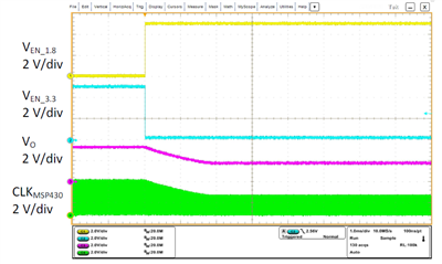 Figure 2 MSP430 Supply Transition from 1.8V to 3.3V
Variable output-voltage level. The Linear Regulator as a Dynamic Voltage Scaling Power Supply Reference Design demonstrates a DVS technique in which I2C commands adjust the output voltage of the LP3878-ADJ adjustable LDO. In this particular application, the output voltage is adjustable from 1.2V to 1.6V, with 4mV steps in-between. Figure 3 shows a simplified block diagram of the design; the TPL0401A I2C digital potentiometer changes the feedback resistance at the ADJ pins of the LDO, thus changing the LDO’s output voltage. Figure 4 shows the relationship between the digital potentiometer resistance and LDO output voltage.
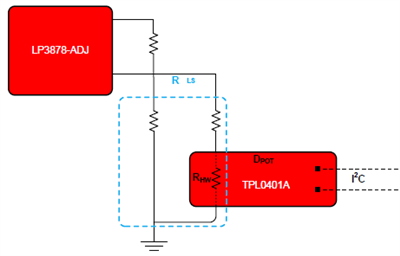 Figure 3 Linear Regulator as a Dynamic Voltage Scaling Power Supply Reference Design Block Diagram
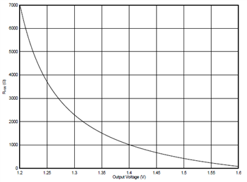 Figure 4 TPL0401A Resistance versus LP3878 Output Voltage
Ultra-low Sleep-mode Current
Figure 5 is a block diagram of the Power Cycling Reference Design to Extend Battery Life Using an Ultra-Low IQ LDO and Nano Timer, which extends battery life by power cycling. Power cycling enables and disables the LDO or power stage to achieve great power savings by taking advantage of the low standby quiescent current of the LDO and nanotimer. The system activates periodically to analyze data, transmit data or execute commands. When the microprocessor completes the process, the system deactivates and enters an ultra-low IQ sleep cycle.
Figure 6 shows the substantial current differences. Over the lifetime of the battery, this savings could mean months or even years.
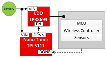 Figure 5 Power Cycling Reference Design to Extend Battery Life Using an Ultra-Low IQ LDO and Nano Timer Block Diagram
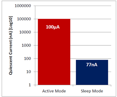 Figure 6 Comparison between Sleep Mode and Active Mode
LDOs are the number-one pick for low-noise, easy to implement small size power solutions. Thanks to their low quiescent current, they can also positively contribute to power efficiency when utilizing the right technique.
Additional Resources:
Jump-start your design with these TI Designs reference designs:
- Linear Regulator Power Solution Reference Design for Reducing MSP430G2xx3 Power TI Design.
- Power Cycling Reference Design to Extend Battery Life Using an Ultra-Low IQ LDO and Nano Timer.
- Linear Regulator as a Dynamic Voltage Scaling Power Supply Reference Design.
- Dynamic Voltage Scaling with a Dual LDO.
- Read the part one and two of the “Drive MSP430 low-power even lower” Power House blog series.