SSZTC00 October 2015 CSD18563Q5A , LMG5200 , TPS40170
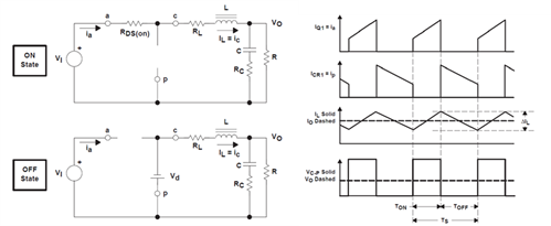
As power engineers, we can recall our first exposure to the idealized buck and boost power stages. Remember how the voltage and current waveforms were nice and simple (Figure 1), and how it was easy to calculate average values and determine the transfer functions relating inputs and outputs?
 Figure 1 The Idealized Buck and Boost
Power Stages: These Look Great!
Figure 1 The Idealized Buck and Boost
Power Stages: These Look Great!As we learned more about implementing converters with practical components, the waveforms got a lot more complicated. One particular no ideality that continues to plague switching converters is the reverse recovery of the MOSFET body diode used in synchronous buck or boost converters. Gallium nitride- GaN- devices do not exhibit the reverse-recovery characteristic, and thus avoid the losses and other associated problems. With my LMG5200 EVM and a comparative silicon FET-based TPS40170EVM-597, I’ll set out to measure reverse recovery in a 24V to 5V / 4A power converter.
Reverse Recovery – What Is It?
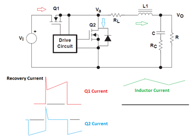
Reverse recovery in a diode is the flow of reverse current (the wrong way!) through the diode as reverse voltage is applied across the terminals (see Figure 2). There is stored charge in the diode that must recombine before the diode can block reverse voltage. This recombination is a function of temperature, forward current, Ifwd, di/dt of the current and other factors.
 Figure 2 Reverse Recovery Current Waveforms
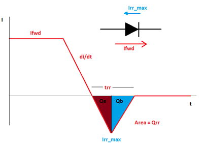
Recovered charge, Qrr, is split into two components: Qa before recovery and Qb after recovery – where the diode starts supporting reverse voltage – see Figure 3. You may see soft recovery where the Qb is about the same as Qa so that -di/dt is slow, or you may see “snappy” diodes where Qb is very small and -di/dt is very high. With high -di/dt (due to a diode snapping off), the parasitic inductances in the bridge power loop respond by dumping their stored energy into the parasitic-node capacitances; voltage ringing occurs due to the second-order response. This is one good reason to place the input power-stage bypass capacitors close to the input stage. With less inductance in the loop for a snappy recovery, there is less energy to cause voltage ringing with the parasitic capacitances.
 Figure 3 Recovered Charge
I account for reverse recovery loss in the conventional way: I take Qrr as specified in the data sheet and multiply by the frequency and input voltage (for a buck converter) or output voltage (for a boost converter). Diode or MOSFET data sheets typically specify a reverse-recovery time and a reverse-recovery charge. For instance, the CSD18563Q5A specifies a reverse recovery time, trr, of 49ns and a Qrr of 63nC. Equation 1 calculates the first-order estimate of the loss due to Qrr for a 300kHz, 24V-> 5V buck converter as:
Qrr Loss ~24V * 300kHz * 63nC = 454mW (1)
Be warned! The Qrr is typically specified at 25°C for a particular Ifwd and di/dt. The actual Qrr could double (or more) at elevated junction temperatures such as 125°C. The di/dt and initial current both have an impact (higher or lower). For snappy diodes, most of this power is dissipated in the upper switch. For soft-recovery diodes, the power splits between the upper switch and the body diode. I use twice the 25°C losses as a better estimate for recovery-related losses if the di/dt and Ifwd conditions are similar to my application.
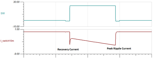
So how do you plan for those losses? What is the real peak current due to reverse recovery in the actual circuit? You might be tempted to use a SPICE tool to simulate the recovery, but I have not seen good models for diode recovery in the SPICE community. Figure 4 shows the results of a TINA-TI™ simulation that I modified from the TPS40170 product folder of our 24V/5V buck converter, showing the switch-node voltage (SW) and current in the top switch (load current plus reverse-recovery current and switch-node capacitance current sensed with a 10mΩ shunt).
 Figure 4 TINA-TI™ Simulation: TPS540170
Notice the ~5A peak ripple current and 5A peak reverse recovery plus the switch-node capacitance charging current. I ran the simulation and increased the temperature from 27°C to 125°C – the peak recovery current didn’t increase – and it didn’t seem that SPICE was correctly modeling the recovery.
In part 2 of this series, I’ll detail a method for measuring reverse recovery in an actual circuit and then compare a standard MOSFET-based synchronous buck converter to the new LMG5200.