SSZTD11 November 2023 AM263P2-Q1 , AM263P4 , AM263P4-Q1 , UCC5880-Q1 , UCC5881-Q1
A traction inverter converts the EV battery’s high-voltage DC to the AC that the electric motor needs. The traction inverter controls the speed and torque of the motor, and its efficiency has a direct impact on the power and thermal dissipation, as well the EV’s driving range.
Figure 1 shows some of the most important components for the traction inverter: the microcontroller (MCU), isolated gate driver, and isolated bias supply chip or module.
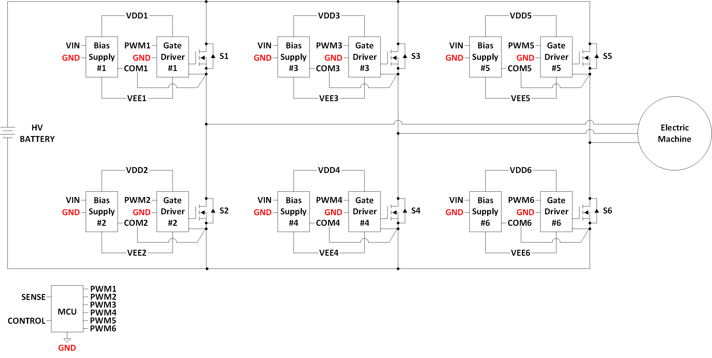 Figure 1 EV traction inverter block
diagram
Figure 1 EV traction inverter block
diagramTo maximize reliability and efficiency in traction inverters, you’ll have to tackle design challenges related to each of these three components. Let’s look at innovations that are helping mitigate these challenges.
Component No. 1: A real-time control MCU
Dropping both EV traction inverter size and weight to increase driving range and reduce costs puts new demands on the MCU. One way to reduce size and weight is spin the motor at higher speeds (>20 kRPM), but to do so requires optimizing the control loop for low latency, from analog-to-digital converter (ADC) read, to field-oriented control (FOC) computing, to pulse-width modulation (PWM) write.
TI has many accelerators and features to achieve low control-loop latency including some specifically designed for traction inverters. Two such accelerators on the AM263P4-Q1 MCU are the resolver-to-digital converter (RDC) and trigonometric math unit (TMU).
The RDC converts sine/cosine feedback from the resolver sensor and to speed and position. This computation occurs in dedicated hardware in order to speed up the conversion process and offload this function from the main cores. Other diagnostic features built into TI MCUs include the sin2 + cos2 = 1 check. Combining these diagnostics with two redundant RDCs creates an optimized solution for traction inverters that must meet Automotive Safety Integrity Level (ASIL) D.
The TMU coprocessor runs parallel to every core and offloads trigonometric math functions from the main cores, while also providing improvements up to 8times the speed of these functions. The increased speed provides significant control-loop benefits to traction inverters, since most traction inverter control loops use FOC algorithms implementing Clarke and Park transformations that require trigonometric math functions.
The RDC and TMU accelerators, including the control subsystem, result in a real-time control latency of <3 µs, enabling control of high-speed traction inverter motors well beyond 20 kRPM, and thus the ability to reduce system size and weight.
Component No. 2: Gate drivers
As traction inverter power levels approach 500 kW, improving efficiency (reducing energy losses throughout the drive cycle) is the primary gate-driver design consideration. Other design requirements include power density, weight, height, functional safety and cost.
To improve efficiency, the industry has widely adopted silicon carbide (SiC) field-effect transistors (FETs); the isolated gate drivers powering these switches have become more sophisticated, and now include isolated ADC sensing, multiple modes of overcurrent protection, bias supply monitoring, gate monitoring, programmable safe states, built-in self-test, and a new feature called real-time variable gate-drive strength.
Depending on safety requirements of the system, having a functional safety-compliant gate-driver integrated circuit (IC) helps to support the system achieve International Organization for Standardization 26262 compliance. For example, the gate driver can help ensure ASIL-D fault detection of ≥99% and ≥90% for single and latent faults, respectively.
Modern gate-driver ICs turn the SiC FETs on and off as quickly as possible through a voltage slew-rate control method (transient voltages), minimizing the “time = dt component,” reducing turnon and turnoff energy, and thus reducing overall switching losses. This ability to control and vary the gate-drive current strength provides an impressive reduction in switching losses, but at the expense of increasing transient overshoot at the switch node during switching, as shown in Figure 2.
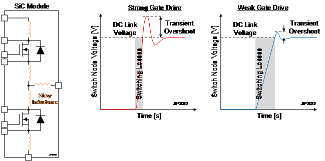 Figure 2 SiC slew-rate control by
varying gate-driver IC drive strength
Figure 2 SiC slew-rate control by
varying gate-driver IC drive strengthReal-time variable gate-drive strength offers the ultimate flexibility to optimize traction inverter designs for both efficiency and transient overshoot mitigation.
Looking at an EV battery charging cycle, SiC transient overshoot reduction and efficiency optimization are possible, with three-fourths of the charge cycle available for efficiency improvements; see Figure 3.
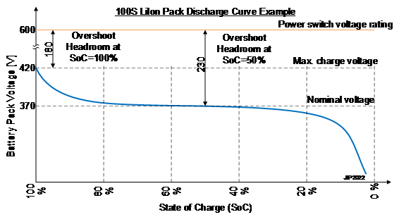 Figure 3 Efficiency zone during battery
peak voltage vs. state of charge
Figure 3 Efficiency zone during battery
peak voltage vs. state of chargeThe functional safety-compliant UCC5880-Q1 gate driver helps achieve efficiency gains with a dual-output, split-output structure and a variable current strength configuration through a 4-MHz bidirectional Serial Peripheral Interface (SPI) bus, or three digital input pins if you don’t want to use the SPI bus to set the drive strength at power-up.
Component No. 3: The bias supply
An EV requires efficient power conversion from the traction inverter to enable longer battery run times through each full discharge cycle. The isolated gate-driver bias supply plays a role in achieving high efficiency by minimizing the conduction power losses of SiC power modules. Setting the gate voltage to the maximum allowable level reduces the drain-to-source on-resistance (RDS(on)), while ensuring reliability (Figure 4). Reducing RDS(on) is important as currents approach and exceed 400 A in traction inverters, making Idson 2 ´ RDS(on) conduction power losses excessive.
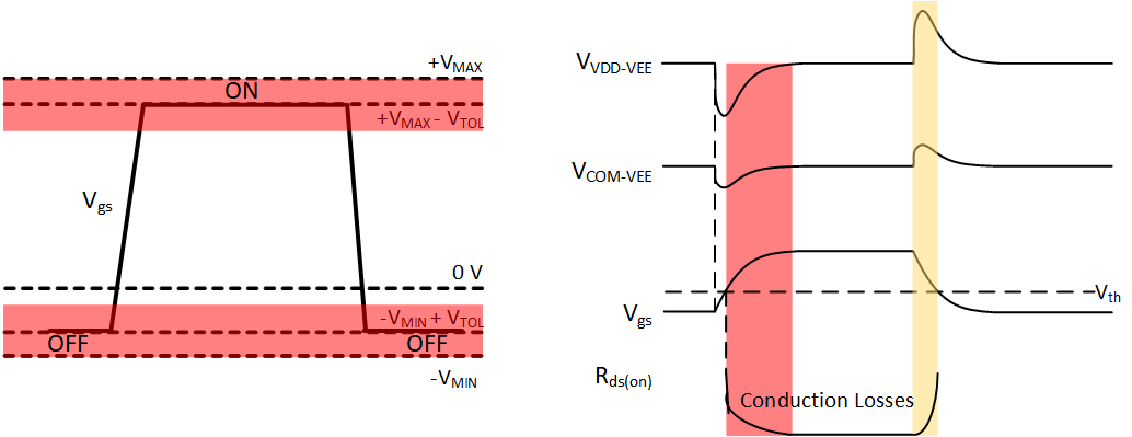 Figure 4 SiC gate-source voltage limits
and conduction losses during a switching cycle
Figure 4 SiC gate-source voltage limits
and conduction losses during a switching cycleTI isolated DC/DC bias modules minimize conduction losses, while the UCC5880-Q1 minimizes switching losses. Both positive and negative gate-drive rail voltages are easily adjustable at the most efficient gate voltage setting for either SiC or IGBT drives, with an accuracy of <1.3% over full operating conditions (voltage, safe operating area power, temperature and process). The closed-loop feedback provides high-accuracy regulation for gate-drive voltage control, maximizing safety and efficiency of the SiC or insulated-gate bipolar transistor module.
TI isolated DC/DC bias modules provide a high-density solution, integrating the isolation power transformer, primary-side bridge, secondary-side bridge and control logic. The small package footprint enables an efficient, small driving solution in multiphase traction inverters through a >30% smaller printed circuit board area, <4-mm height, and the elimination of over 30 discrete components, improving the failure-in-time rate (Figure 5).
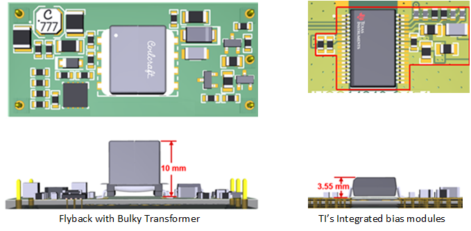 Figure 5 A TI isolated bias module vs.
flyback size and component comparison
Figure 5 A TI isolated bias module vs.
flyback size and component comparisonConclusion
Next-generation traction inverters can operate at efficiencies up to 5% higher and achieve higher speeds, higher power density, lower height, lower weight and lower system costs. Traction inverters continue to develop in these areas as the EV market accelerates with new manufacturers launching new models to take market share from established leaders.