SWRA495K December 2015 – April 2024 CC1310 , CC1350 , CC2620 , CC2630 , CC2640 , CC2640R2F , CC2640R2F-Q1 , CC2642R-Q1 , CC2650 , CC2662R-Q1
- 1
- Abstract
- Trademarks
- 1Oscillator and Crystal Basics
- 2Overview of Crystal Oscillators for CC devices
- 3Selecting Crystals for the CC devices
- 4PCB Layout of the Crystal
- 5Measuring the Amplitude of the Oscillations of Your Crystal
- 6Crystals for CC13xx, CC26xx and CC23xx
- 7High Performance BAW Oscillator
- 8References
- 9Revision History
4 PCB Layout of the Crystal
The layout of the crystal can reduce the parasitic capacitance and, more importantly, reduce noise from coupling on the input of the oscillators. Noise on the input of the oscillator can lead to severe side effects such as clock glitches, flash corruption, or system crashes because the CC26xx and CC13xx devices rely on the crystal oscillators as the high- and low-frequency system clock.
The following are a few recommendations for the layout of the crystals:
- Place the crystal as close as possible to the device to minimize the length of the PCB traces. (This placement reduces crosstalk and minimizes EMI.)
- TI recommends a solid ground plane under the crystal.
- Ensure no high-speed digital signals are close to the crystal to minimize cross-coupling of noise into the oscillator.
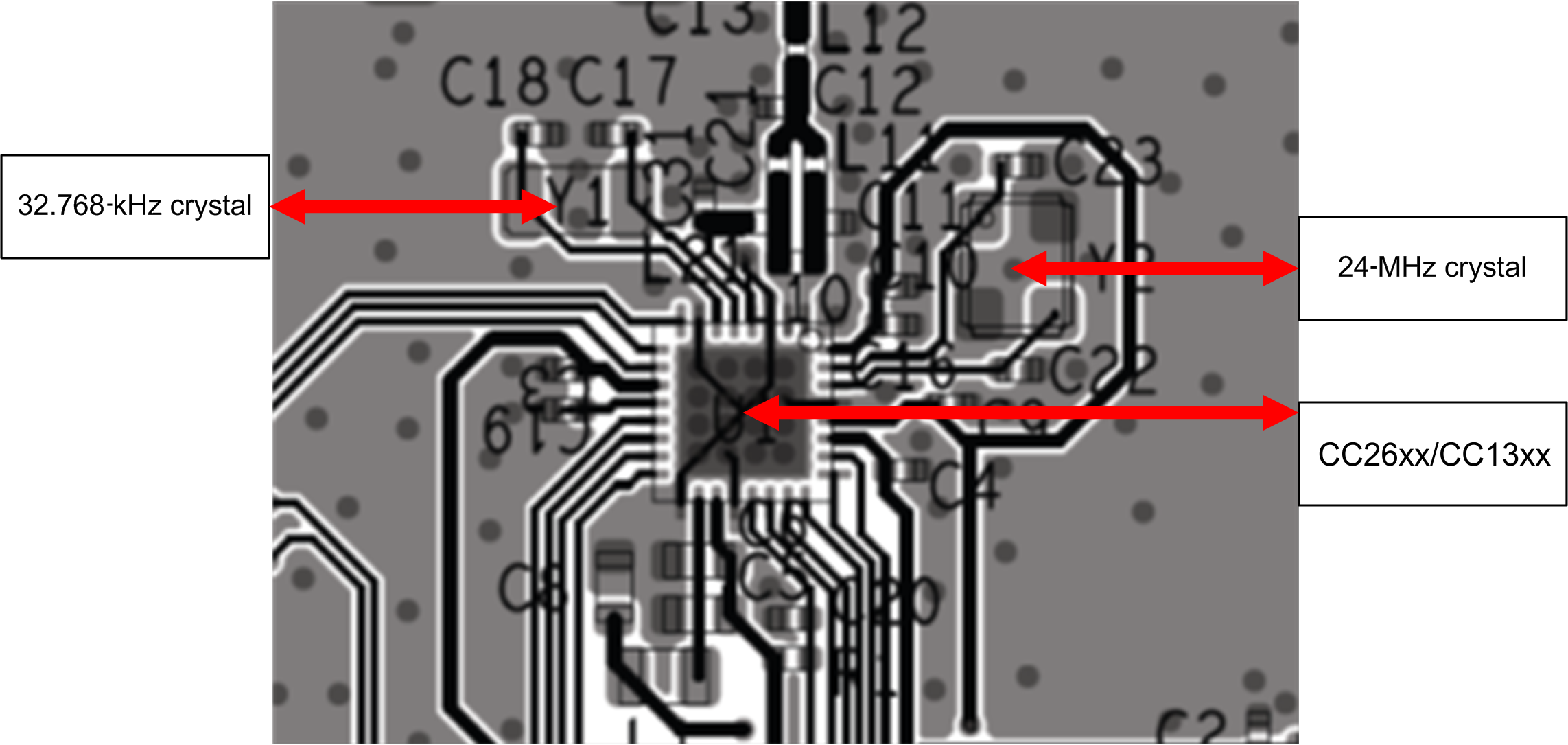
Figure 4-1 shows the top layer of the layout of the CC26xx reference design. The bottom layer is a solid ground plane. For more details, see the SimpleLink™ CC2650 EVM Kit 4XD (CC2650EM-4XD) v1.0.3 Design Files. The same crystal layout can be used with CC13xx device.
 Figure 4-1 Layout of the CC26xx EVM