SWRS202C May   2017  – January 2022 AWR1443

PRODUCTION DATA  

  1. Features
  2. Applications
  3. Description
  4. Functional Block Diagram
  5. Revision History
  6. Device Comparison
    1. 6.1 Related Products
  7. Terminal Configuration and Functions
    1. 7.1 Pin Diagram
    2. 7.2 Signal Descriptions
      1. 7.2.1 Signal Descriptions
    3. 7.3 Pin Multiplexing
  8. Specifications
    1. 8.1 Absolute Maximum Ratings
    2. 8.2 ESD Ratings
    3. 8.3 Power-On Hours (POH)
    4. 8.4 Recommended Operating Conditions
    5. 8.5 Power Supply Specifications
    6. 8.6 Power Consumption Summary
    7. 8.7 RF Specification
    8. 8.8 Thermal Resistance Characteristics for FCBGA Package [ABL0161]
    9. 8.9 Timing and Switching Characteristics
      1. 8.9.1  Power Supply Sequencing and Reset Timing
      2. 8.9.2  Synchronized Frame Triggering
      3. 8.9.3  Input Clocks and Oscillators
        1. 8.9.3.1 Clock Specifications
      4. 8.9.4  Multibuffered / Standard Serial Peripheral Interface (MibSPI)
        1. 8.9.4.1 Peripheral Description
        2. 8.9.4.2 MibSPI Transmit and Receive RAM Organization
          1. 8.9.4.2.1 SPI Timing Conditions
          2. 8.9.4.2.2 SPI Controller Mode Switching Parameters (CLOCK PHASE = 0, SPICLK = output, SPISIMO = output, and SPISOMI = input) (1) (1) (1)
          3. 8.9.4.2.3 SPI Controller Mode Switching Parameters (CLOCK PHASE = 1, SPICLK = output, SPISIMO = output, and SPISOMI = input) (1) (1) (1)
        3. 8.9.4.3 SPI Peripheral Mode I/O Timings
          1. 8.9.4.3.1 SPI Peripheral Mode Switching Parameters (SPICLK = input, SPISIMO = input, and SPISOMI = output) (1) (1) (1)
        4. 8.9.4.4 Typical Interface Protocol Diagram (Peripheral Mode)
      5. 8.9.5  LVDS Interface Configuration
        1. 8.9.5.1 LVDS Interface Timings
      6. 8.9.6  General-Purpose Input/Output
        1. 8.9.6.1 Switching Characteristics for Output Timing versus Load Capacitance (CL)
      7. 8.9.7  Controller Area Network Interface (DCAN)
        1. 8.9.7.1 Dynamic Characteristics for the DCANx TX and RX Pins
      8. 8.9.8  Serial Communication Interface (SCI)
        1. 8.9.8.1 SCI Timing Requirements
      9. 8.9.9  Inter-Integrated Circuit Interface (I2C)
        1. 8.9.9.1 I2C Timing Requirements (1)
      10. 8.9.10 Quad Serial Peripheral Interface (QSPI)
        1. 8.9.10.1 QSPI Timing Conditions
        2. 8.9.10.2 Timing Requirements for QSPI Input (Read) Timings (1) (1)
        3. 8.9.10.3 QSPI Switching Characteristics
      11. 8.9.11 JTAG Interface
        1. 8.9.11.1 JTAG Timing Conditions
        2. 8.9.11.2 Timing Requirements for IEEE 1149.1 JTAG
        3. 8.9.11.3 Switching Characteristics Over Recommended Operating Conditions for IEEE 1149.1 JTAG
  9. Detailed Description
    1. 9.1 Overview
    2. 9.2 Functional Block Diagram
    3. 9.3 External Interfaces
    4. 9.4 Subsystems
      1. 9.4.1 RF and Analog Subsystem
        1. 9.4.1.1 Clock Subsystem
        2. 9.4.1.2 Transmit Subsystem
        3. 9.4.1.3 Receive Subsystem
        4. 9.4.1.4 Radio Processor Subsystem
      2. 9.4.2 Main (Control) System
      3. 9.4.3 Host Interface
    5. 9.5 Accelerators and Coprocessors
    6. 9.6 Other Subsystems
      1. 9.6.1 ADC Channels (Service) for User Application
        1. 9.6.1.1 GP-ADC Parameter
    7. 9.7 Boot Modes
      1. 9.7.1 Flashing Mode
      2. 9.7.2 Functional Mode
  10. 10Applications, Implementation, and Layout
    1. 10.1 Application Information
    2. 10.2 Short-Range Radar
    3. 10.3 Blind Spot Detector and Ultrasonic Upgrades
    4. 10.4 Reference Schematic
  11. 11Device and Documentation Support
    1. 11.1 Device Nomenclature
    2. 11.2 Tools and Software
    3. 11.3 Documentation Support
    4. 11.4 Support Resources
    5. 11.5 Trademarks
    6. 11.6 Electrostatic Discharge Caution
    7. 11.7 Glossary
  12. 12Mechanical, Packaging, and Orderable Information
    1. 12.1 Packaging Information

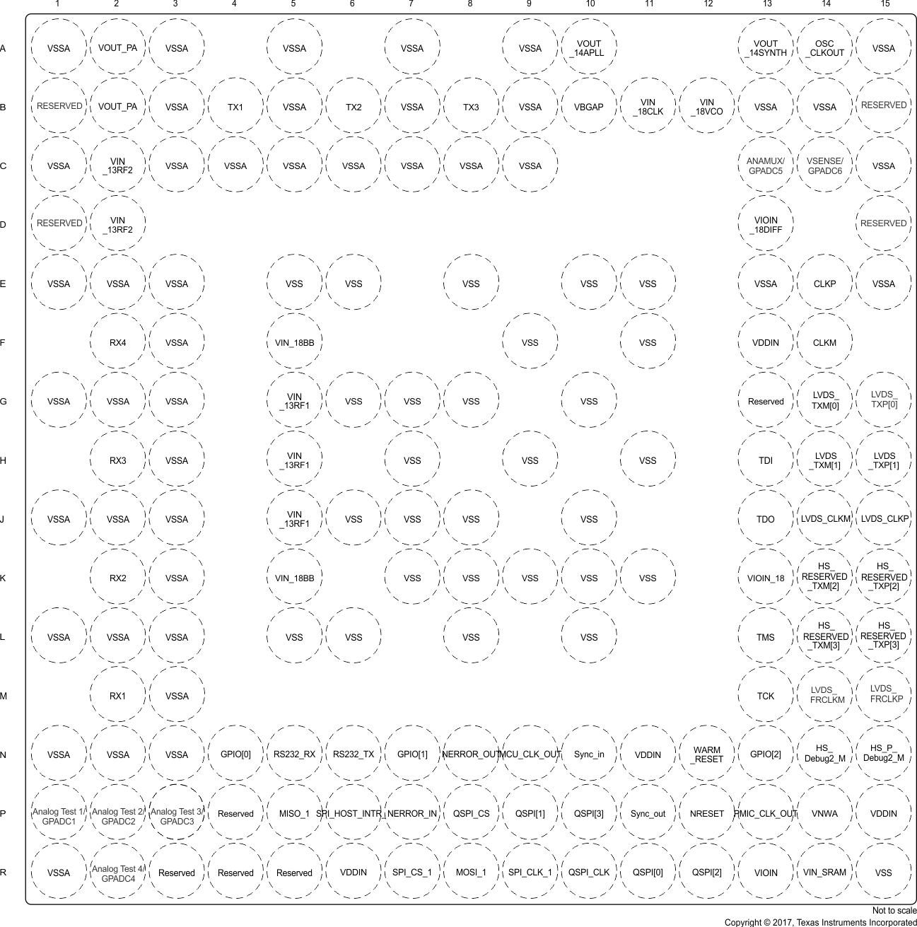
Pin Diagram

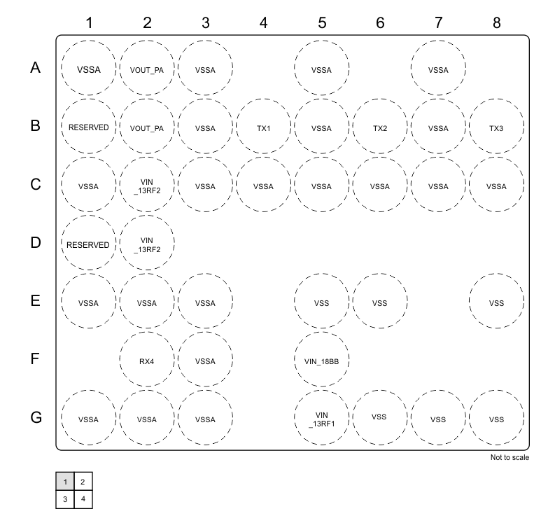
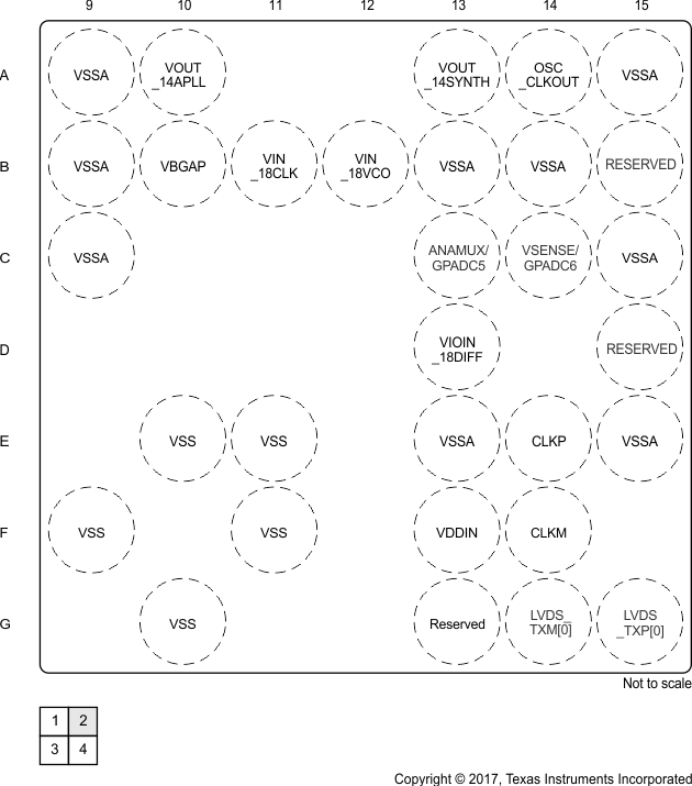
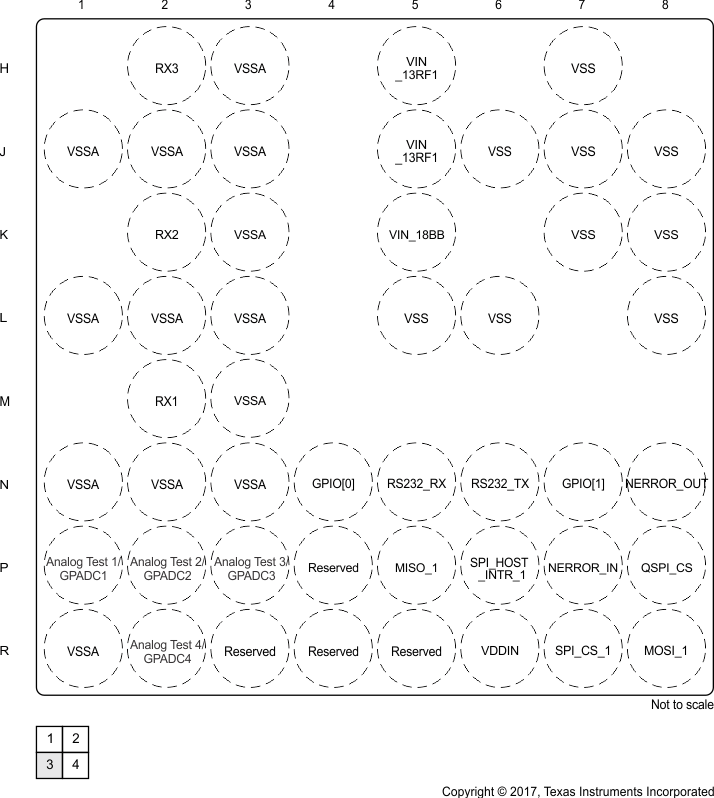
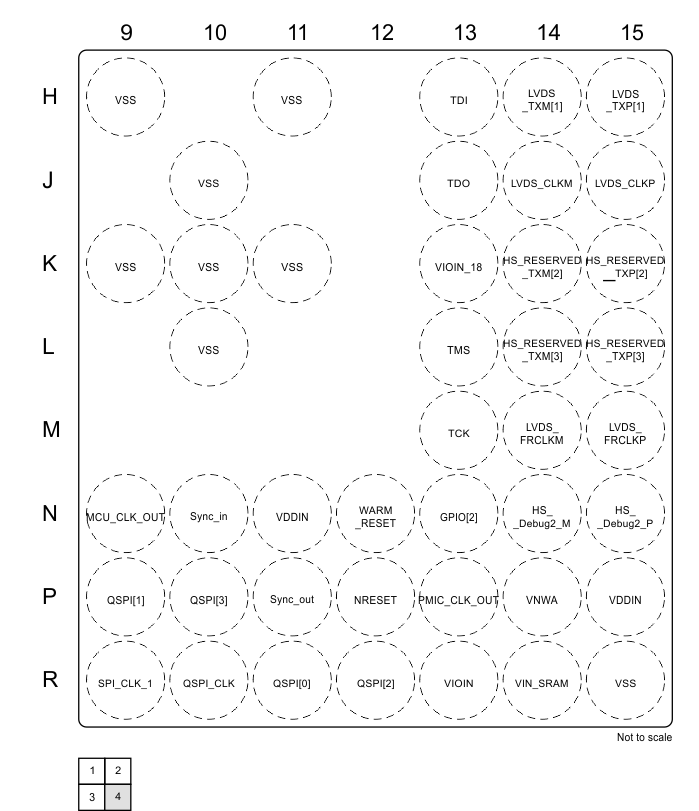
#X4608 shows the pin locations for the 161-pin FCBGA package. #X7702, #X7371, #X7626, and #X8420 show the same pins, but split into four quadrants.

GUID-ABE18BCA-C8A2-4CF1-AAA0-A17DD4BEB2CC-low.gif Figure 7-1 Pin Diagram
GUID-75C3107A-DB63-4262-99F7-B8601C69DBF1-low.gif Figure 7-2 Top Left Quadrant
GUID-A0E0FCAA-79B9-4054-B218-53B8A841E76F-low.gif Figure 7-3 Top Right Quadrant
GUID-7A262515-A78C-4D1D-B0BA-F5EF73DB4716-low.gif Figure 7-4 Bottom Left Quadrant
GUID-97BE8E4C-B8BC-4CBD-94F2-35D887DBB44E-low.gif Figure 7-5 Bottom Right Quadrant