TIDT278 April   2022


  1.   Description
  2.   Features
  3.   Applications
  4. 1Test Prerequisites
    1. 1.1 Voltage and Current Requirements
    2. 1.2 Considerations
    3. 1.3 Dimensions
  5. 2Testing and Results
    1. 2.1 Efficiency Graphs
    2. 2.2 Loss
    3. 2.3 Load Regulation
      1. 2.3.1 5-V Output Voltage
      2. 2.3.2 3.3-V Output Voltage
      3. 2.3.3 12-V Output Voltage
    4. 2.4 Line Regulation
      1. 2.4.1 5-V Outputs
      2. 2.4.2 3.3-V Output Voltage
      3. 2.4.3 12-V Output Voltage
      4. 2.4.4 Efficiency and Loss in Dependance of Input Voltage
    5. 2.5 Cross Regulation Light Load and Full Load
      1. 2.5.1 Bias Current 1 mA
      2. 2.5.2 Bias Current 5 mA
    6. 2.6 Thermal Images
    7. 2.7 Bode Plots
  6. 3Waveforms
    1. 3.1 Switching
      1. 3.1.1 Q1 Drain to GND
      2. 3.1.2 Q1 Gate to GND
      3. 3.1.3 D1 Anode to 12 VOUT
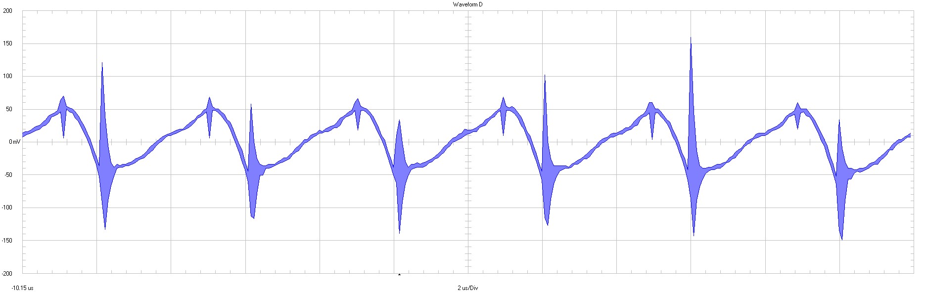
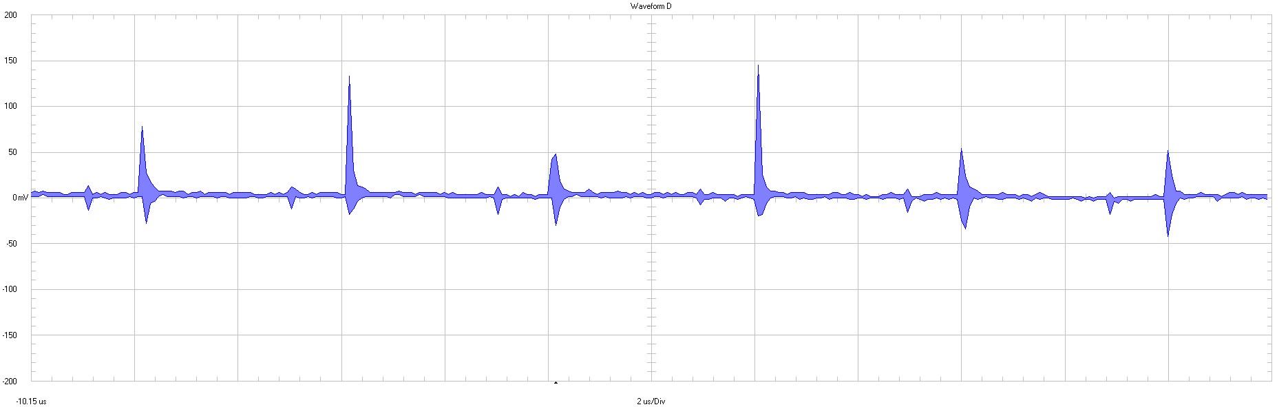
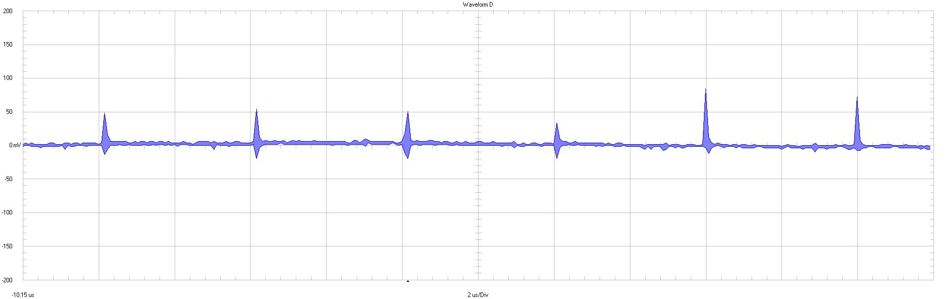
    2. 3.2 Input Voltage Ripple
    3. 3.3 Output Voltage Ripple
      1. 3.3.1 5-V Output Voltage (Primary)
      2. 3.3.2 5-V Output Voltage (Secondary)
      3. 3.3.3 3.3-V Output Voltage
      4. 3.3.4 12-V Output Voltage

Input Voltage Ripple

GUID-20220408-SS0I-LSCC-CQWN-DLZ32FJM9FSQ-low.jpg

Power stage in

50 mV / div

2 µs / div

20 MHz bandwidth

GUID-20220408-SS0I-8D4M-8GHK-MVMGDF4H6VWM-low.jpg

between D9 and L1

50 mV / div

2 µs / div

20 MHz bandwidth

GUID-20220408-SS0I-SSFS-BWBZ-1WHVDGMWKBPB-low.jpg

Jmp1

50 mV / div

2 µs / div

20 MHz bandwidth

Figure 3-4 Input Voltage Ripple

The input filter is attenuating the reflected ripple (= conducted emissions).

To attenuate RF spikes further a ferrite bead (600 Ω at 100 MHz) could be added to the input.

GUID-20220408-SS0I-3JWH-671M-9GQBXNWF8GWF-low.jpg

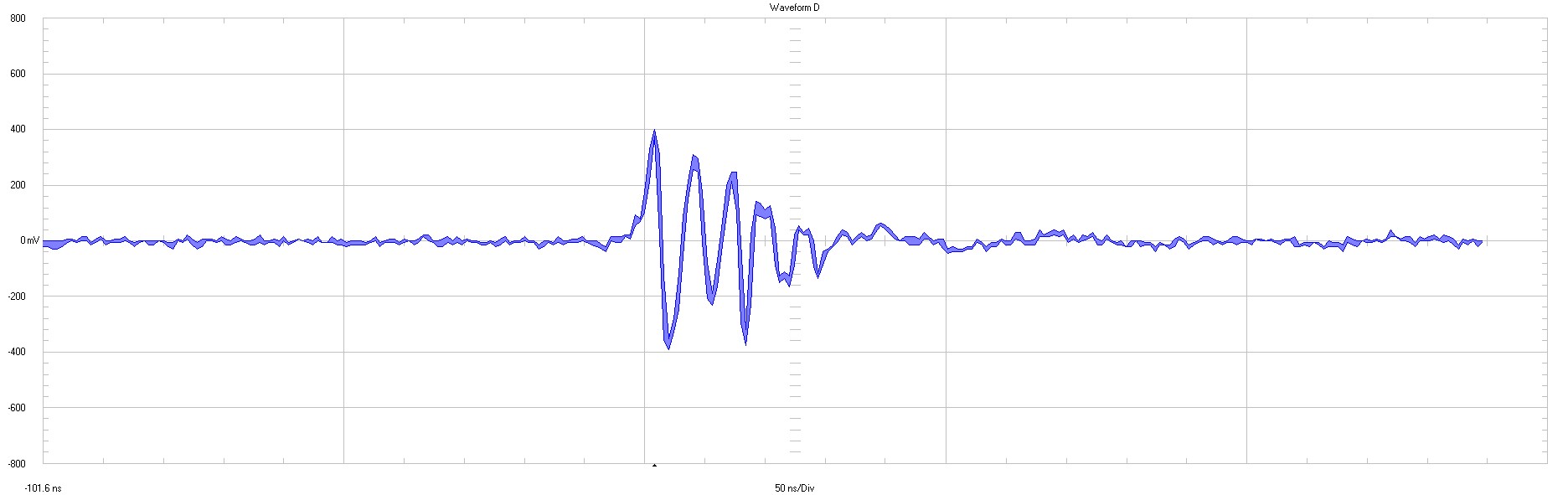
Jmp1

200 mV / div

50 ns / major div

full bandwidth

Figure 3-5 Input Ripple (Jmp1 Zoomed and Full Bandwidth)