TIDT278 April   2022


  1.   Description
  2.   Features
  3.   Applications
  4. 1Test Prerequisites
    1. 1.1 Voltage and Current Requirements
    2. 1.2 Considerations
    3. 1.3 Dimensions
  5. 2Testing and Results
    1. 2.1 Efficiency Graphs
    2. 2.2 Loss
    3. 2.3 Load Regulation
      1. 2.3.1 5-V Output Voltage
      2. 2.3.2 3.3-V Output Voltage
      3. 2.3.3 12-V Output Voltage
    4. 2.4 Line Regulation
      1. 2.4.1 5-V Outputs
      2. 2.4.2 3.3-V Output Voltage
      3. 2.4.3 12-V Output Voltage
      4. 2.4.4 Efficiency and Loss in Dependance of Input Voltage
    5. 2.5 Cross Regulation Light Load and Full Load
      1. 2.5.1 Bias Current 1 mA
      2. 2.5.2 Bias Current 5 mA
    6. 2.6 Thermal Images
    7. 2.7 Bode Plots
  6. 3Waveforms
    1. 3.1 Switching
      1. 3.1.1 Q1 Drain to GND
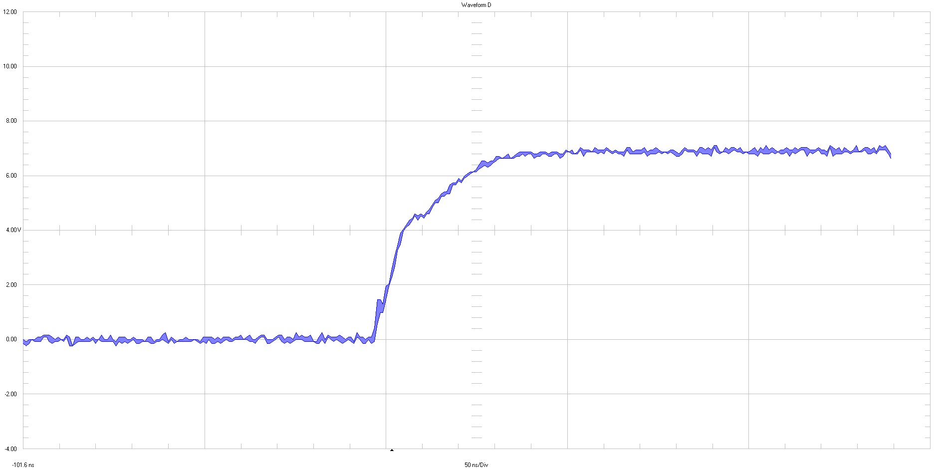
      2. 3.1.2 Q1 Gate to GND
      3. 3.1.3 D1 Anode to 12 VOUT
    2. 3.2 Input Voltage Ripple
    3. 3.3 Output Voltage Ripple
      1. 3.3.1 5-V Output Voltage (Primary)
      2. 3.3.2 5-V Output Voltage (Secondary)
      3. 3.3.3 3.3-V Output Voltage
      4. 3.3.4 12-V Output Voltage

Q1 Gate to GND

GUID-20220408-SS0I-H9DF-SHHS-SF507N9HW5S2-low.jpg

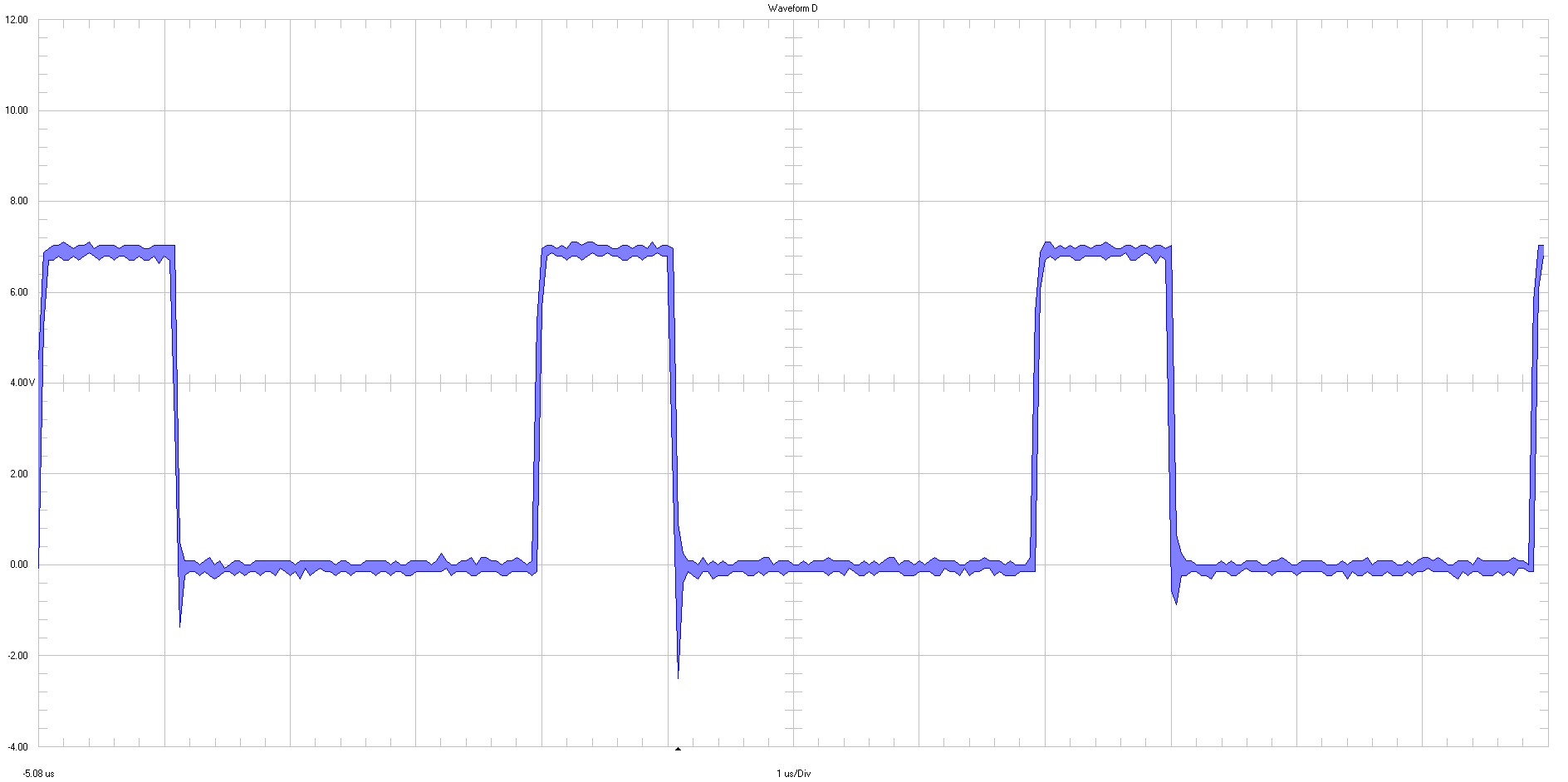
2 V / div

1 µs / div

full bandwidth

GUID-20220408-SS0I-X4XX-TM4B-9JZZJDRKFNNK-low.jpg
GUID-20220408-SS0I-PZND-WKL0-V323W5BS3T3D-low.jpg

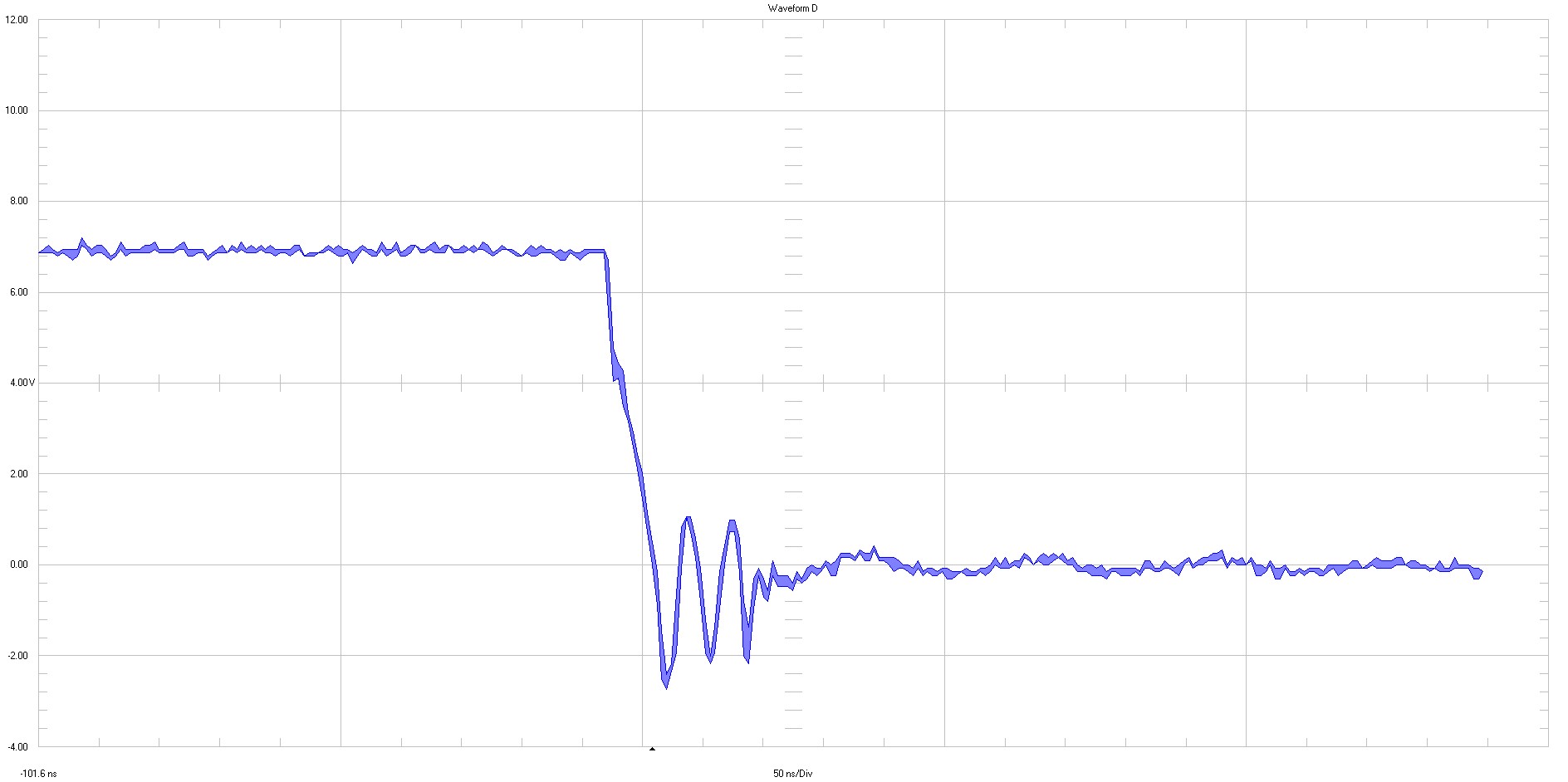
2 V / div

50 ns / major div

full bandwidth

Figure 3-2 Switching (Q1 Gate to GND)