TIDUEP0 May 2020
- Description
- Resources
- Features
- Applications
- 1Design Images
- 2System Description
-
3System Overview
- 3.1 Block Diagram
- 3.2 Design Considerations
- 3.3
Highlighted Products
- 3.3.1 TPD4E05U06 4-Channel Ultra-Low-Capacitance IEC ESD Protection Diode
- 3.3.2 TPD2EUSB30 2-Channel ESD Solution for SuperSpeed USB 3.0 Interface
- 3.3.3 2.3.3 HD3SS3220 10Gbps USB 3.1 USB Type-C 2:1 MUX With DRP Controller
- 3.3.4 TPS54218 2.95V to 6V Input, 2A Synchronous Step-Down SWIFT™ Converter
- 3.3.5 TPS54318 2.95V to 6V Input, 3A Synchronous Step-Down SWIFT™ Converter
- 3.3.6 CSD19538Q3A 100V, N ch NexFET MOSFET™, single SON3x3, 49mOhm
- 3.3.7 LM3488 2.97V to 40V Wide Vin Low-Side N-Channel Controller for Switching Regulators
- 3.3.8 TPS61178 20-V Fully Integrated Sync Boost with Load Disconnect
- 3.3.9 LMZM23601 36-V, 1-A Step-Down DC-DC Power Module in 3.8-mm × 3-mm Package
- 3.3.10 TPS7A39 Dual, 150mA, Wide-Vin, Positive and Negative Low-Dropout (LDO) Voltage Regulator
- 3.3.11 TPS74201 Single-output 1.5-A LDO regulator, adjustable (0.8V to 3.3V), any or no cap, programmable soft start
- 3.3.12 LP5910 300-mA low-noise low-IQ low-dropout (LDO) linear regulator
- 3.3.13 LP5907 250-mA ultra-low-noise low-IQ low-dropout (LDO) linear
- 3.3.14 INA231 28V, 16-bit, i2c output current/voltage/power monitor w/alert in wcsp
- 3.4
System Design Theory
- 3.4.1 Input Section
- 3.4.2
Designing of SEPIC based High Voltage Supply
- 3.4.2.1 Basic Operation Principle of SEPIC Converter
- 3.4.2.2 Design of Dual SEPIC Supply using uncoupled inductors
- 3.4.2.3 Duty Cycle
- 3.4.2.4 Inductor Selection
- 3.4.2.5 Power MOSFET Selection
- 3.4.2.6 Output Diode Selection
- 3.4.2.7 Coupling Capacitor Selection
- 3.4.2.8 Output Capacitor Selection
- 3.4.2.9 Input Capacitor Selection
- 3.4.2.10 Programming the Output Voltage
- 3.4.3 Designing the Low Voltage Power Supply
- 3.4.4 Designing the TPS54218 through Webench Power Designer
- 3.4.5 ± 5V Transmit Supply Generation
- 3.4.6 System Clock Synchronization
- 3.4.7 Power and data output connector
- 3.4.8 System Current and Power Monitoring
- 4Hardware, Software, Testing Requirements, and Test Results
- 5Layout Guidelines
- 6Design Files
- 7Software Files
- 8Related Documentation
- 9About the Author
4.1.2.3 Load Transient Test
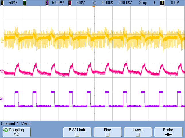
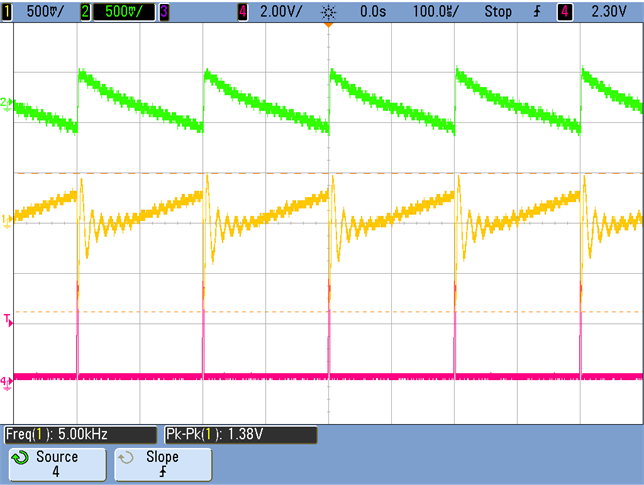
Figure 33 shows the load transient response of the power supply. The load of 25 mA per rail is applied onto both positive and negative rail with a duty cycle 20% at pulse repetition frequency of 5 kHz, as shown in purple waveform. A drop of less than 50 mV is observed on both the rails. Moreover, the load transient response test is repeated in case the load of the power supply is 1 A per rail with a duty cycle of 1%, at pulse repetition frequency of 5 kHz. The result in Figure 34, shows a drop of less than 1 V per rail.
Figure 33. Load Transient Response of Positive and Negative Output Rail With Symmetrical Loads (25 mA)

Figure 34. Load Transient Response of Positive and Negative Output Rail With Symmetrical Loads (1A) 
