TIDUEP0 May 2020
- Description
- Resources
- Features
- Applications
- 1Design Images
- 2System Description
-
3System Overview
- 3.1 Block Diagram
- 3.2 Design Considerations
- 3.3
Highlighted Products
- 3.3.1 TPD4E05U06 4-Channel Ultra-Low-Capacitance IEC ESD Protection Diode
- 3.3.2 TPD2EUSB30 2-Channel ESD Solution for SuperSpeed USB 3.0 Interface
- 3.3.3 2.3.3 HD3SS3220 10Gbps USB 3.1 USB Type-C 2:1 MUX With DRP Controller
- 3.3.4 TPS54218 2.95V to 6V Input, 2A Synchronous Step-Down SWIFT™ Converter
- 3.3.5 TPS54318 2.95V to 6V Input, 3A Synchronous Step-Down SWIFT™ Converter
- 3.3.6 CSD19538Q3A 100V, N ch NexFET MOSFET™, single SON3x3, 49mOhm
- 3.3.7 LM3488 2.97V to 40V Wide Vin Low-Side N-Channel Controller for Switching Regulators
- 3.3.8 TPS61178 20-V Fully Integrated Sync Boost with Load Disconnect
- 3.3.9 LMZM23601 36-V, 1-A Step-Down DC-DC Power Module in 3.8-mm × 3-mm Package
- 3.3.10 TPS7A39 Dual, 150mA, Wide-Vin, Positive and Negative Low-Dropout (LDO) Voltage Regulator
- 3.3.11 TPS74201 Single-output 1.5-A LDO regulator, adjustable (0.8V to 3.3V), any or no cap, programmable soft start
- 3.3.12 LP5910 300-mA low-noise low-IQ low-dropout (LDO) linear regulator
- 3.3.13 LP5907 250-mA ultra-low-noise low-IQ low-dropout (LDO) linear
- 3.3.14 INA231 28V, 16-bit, i2c output current/voltage/power monitor w/alert in wcsp
- 3.4
System Design Theory
- 3.4.1 Input Section
- 3.4.2
Designing of SEPIC based High Voltage Supply
- 3.4.2.1 Basic Operation Principle of SEPIC Converter
- 3.4.2.2 Design of Dual SEPIC Supply using uncoupled inductors
- 3.4.2.3 Duty Cycle
- 3.4.2.4 Inductor Selection
- 3.4.2.5 Power MOSFET Selection
- 3.4.2.6 Output Diode Selection
- 3.4.2.7 Coupling Capacitor Selection
- 3.4.2.8 Output Capacitor Selection
- 3.4.2.9 Input Capacitor Selection
- 3.4.2.10 Programming the Output Voltage
- 3.4.3 Designing the Low Voltage Power Supply
- 3.4.4 Designing the TPS54218 through Webench Power Designer
- 3.4.5 ± 5V Transmit Supply Generation
- 3.4.6 System Clock Synchronization
- 3.4.7 Power and data output connector
- 3.4.8 System Current and Power Monitoring
- 4Hardware, Software, Testing Requirements, and Test Results
- 5Layout Guidelines
- 6Design Files
- 7Software Files
- 8Related Documentation
- 9About the Author
2 System Description
Ultrasound imaging is a widely used technique for diagnostic purpose. In addition to high-performance cart-based ultrasound systems, it is now possible to use a handheld device (smart probe) to accomplish high-quality ultrasound imaging. These smart probes leverage the power and resources of a mobile/tablet to process and display ultrasound images. A typical use case for these systems is to bring modern medical imaging technology to remote places, making the diagnostics faster and much more efficient. This small equipment is typically powered by battery (1S/2S), or from USB source. The data can be transferred over USB or Wi-Fi®.
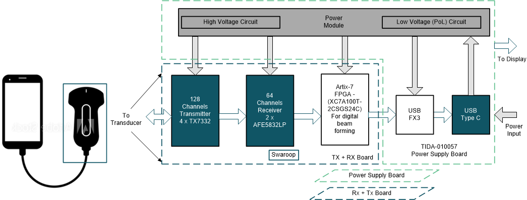
Figure 1 (left) shows a generic picture of such smart probe ultrasound scanner depicting a probe connected to a mobile device. Figure 1 (right) shows the block diagram of the smart probe, which includes transmit (TX) and receive (RX) analog front end (AFEs) for transmitting and receiving ultrasonic pulses and a FPGA to perform beam-forming. The whole setup is powered through the power supply board, consisting of DC-DC converters to generate point of load voltages, HV circuit for powering the transmit chip TX7332 (used in the design) and USB controller for data and power management.

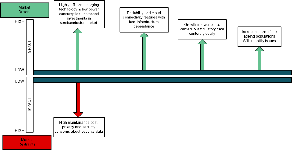
One use case for these systems is to bring modern medical imaging technology to remote villages in developing countries for the first time. Smart ultrasound probes, or ultra-portable ultrasound systems, are the perfect fit for this task due to their cost-effectiveness. The day is fast approaching when most doctors will carry a smart probe unit in their pockets, similar to their stethoscope, by which they can not only hear, but also see inside the body—potentially leading to a market of a few million units worldwide within the next decade, complementing standard ultrasound systems. Figure 2 shows the factors that are the leading reasons for boom in Smart Probe market
