TIDUEP0 May 2020
- Description
- Resources
- Features
- Applications
- 1Design Images
- 2System Description
-
3System Overview
- 3.1 Block Diagram
- 3.2 Design Considerations
- 3.3
Highlighted Products
- 3.3.1 TPD4E05U06 4-Channel Ultra-Low-Capacitance IEC ESD Protection Diode
- 3.3.2 TPD2EUSB30 2-Channel ESD Solution for SuperSpeed USB 3.0 Interface
- 3.3.3 2.3.3 HD3SS3220 10Gbps USB 3.1 USB Type-C 2:1 MUX With DRP Controller
- 3.3.4 TPS54218 2.95V to 6V Input, 2A Synchronous Step-Down SWIFT™ Converter
- 3.3.5 TPS54318 2.95V to 6V Input, 3A Synchronous Step-Down SWIFT™ Converter
- 3.3.6 CSD19538Q3A 100V, N ch NexFET MOSFET™, single SON3x3, 49mOhm
- 3.3.7 LM3488 2.97V to 40V Wide Vin Low-Side N-Channel Controller for Switching Regulators
- 3.3.8 TPS61178 20-V Fully Integrated Sync Boost with Load Disconnect
- 3.3.9 LMZM23601 36-V, 1-A Step-Down DC-DC Power Module in 3.8-mm × 3-mm Package
- 3.3.10 TPS7A39 Dual, 150mA, Wide-Vin, Positive and Negative Low-Dropout (LDO) Voltage Regulator
- 3.3.11 TPS74201 Single-output 1.5-A LDO regulator, adjustable (0.8V to 3.3V), any or no cap, programmable soft start
- 3.3.12 LP5910 300-mA low-noise low-IQ low-dropout (LDO) linear regulator
- 3.3.13 LP5907 250-mA ultra-low-noise low-IQ low-dropout (LDO) linear
- 3.3.14 INA231 28V, 16-bit, i2c output current/voltage/power monitor w/alert in wcsp
- 3.4
System Design Theory
- 3.4.1 Input Section
- 3.4.2
Designing of SEPIC based High Voltage Supply
- 3.4.2.1 Basic Operation Principle of SEPIC Converter
- 3.4.2.2 Design of Dual SEPIC Supply using uncoupled inductors
- 3.4.2.3 Duty Cycle
- 3.4.2.4 Inductor Selection
- 3.4.2.5 Power MOSFET Selection
- 3.4.2.6 Output Diode Selection
- 3.4.2.7 Coupling Capacitor Selection
- 3.4.2.8 Output Capacitor Selection
- 3.4.2.9 Input Capacitor Selection
- 3.4.2.10 Programming the Output Voltage
- 3.4.3 Designing the Low Voltage Power Supply
- 3.4.4 Designing the TPS54218 through Webench Power Designer
- 3.4.5 ± 5V Transmit Supply Generation
- 3.4.6 System Clock Synchronization
- 3.4.7 Power and data output connector
- 3.4.8 System Current and Power Monitoring
- 4Hardware, Software, Testing Requirements, and Test Results
- 5Layout Guidelines
- 6Design Files
- 7Software Files
- 8Related Documentation
- 9About the Author
3 System Overview
There is a growing interest in a hand-held ultrasound system in order to help maximize the effectiveness of point-of-care support and diagnosis for patients . Traditionally, ultrasound systems are of a cart based type, which integrates a higher number of channels to achieve higher performance and superior image quality.
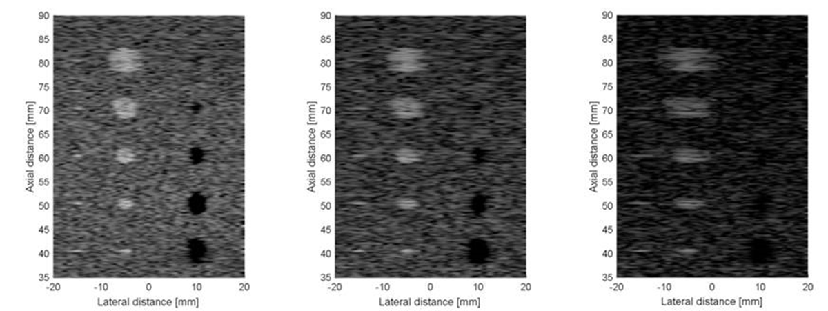
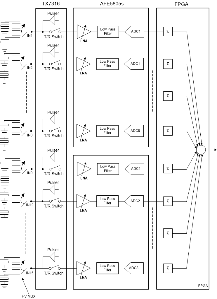
Ultrasound analog front ends and transmitter chips have achieved over 80% reductions in power and size. These advancements allow for higher channel integration and the lowest power possible, which is a must requirement for hand held portable probes since they are typically battery operated (1S/2S). Higher receiver and transmitter channel count in the system gives a better image resolution. Figure 3 show the image quality difference between a 16-CH, 32-CH and a 64-CH system. Because of the power and area limitation in portable ultrasound systems, most of systems in the market are able to integrate 16 or 32 channel receivers and transmitters. The high voltage MUX is used to excite 128 transducer elements; see Figure 4. Some of the limitations for the existing solution are a lower image quality because of only a 16 channel receiver and a lower frame rate because of higher imaging time due to limited number of channels. This reference design proposes a solution which contains a complete power solution for TI’s high performance 128-Ch Tx/64-Ch Rx ultrasound smart probe solution (TX7332+AFE5832LP).


To achieve the target area, all the power supplies and USB Type-C interface are kept on another PCB which is vertically stacked to Rx + Tx board through connector. The other advantage of having power supplies and USB Type-C interface on separate PCB is that it increases isolation of switching noise from power supply and USB Type-C to sensitive receiver and transmitter devices. This power supply board generates a total of 11 different supplies (Including ±80 V) from USB Type-C 5 V with a capability of delivering maximum 15W peak power. It is usual practice to have a CDC or LMK to generate clock for the system. This approach leads to a higher power consumption and extra space on the board. In the proposed solution, to reduce power and board space, the FPGA itself is used to provide clock to all the chips. The power supply board requires 10 LVDS signals including clock and sync. Each LVDS buffer in the FPGA consumes ~39mW/ch which for all 10 LVDS buffers the total power is 390mW. In ultrasound systems the transmitter is active only for 1% of imaging duration. For rest of the duration, the receiver device receives the echo to form the full image. On the same concept, the transmitter device (TX7332) also kept active only for 1% duration which in order to reduce the clock power further, the LVDS signals going to TX7332 is programmed in tri-state mode for 99% duration. The LVDS buffer power in Tri-state mode is 11 mW/ch making the total power consumption of the clocking scheme 213mW. This is an improvement from a conventional clocking scheme power which is greater than 500mW.