TIDUEZ2 March 2021
2.3.1.3 Processing Chain
An example processing chain for obstacle detection is implemented on the AWR1843AOP EVM. The main processing elements involved in the processing chain consist of the following:
- Front end – Represents the antennas and the analog RF transceiver implementing the FMCW transmitter and receiver with the various hardware-based signal conditioning operations.
- ADC – The ADC is the main element that interfaces to the DSP chain. The ADC output samples are buffered in ADC output buffers for access by the digital part of the processing chain.
- EDMA controller – A user-programmed DMA engine employed to move data from one memory location to another without using another processor. The EDMA can be programed to trigger automatically, and can be configured to reorder some of the data during the movement operations.
- C674 DSP – This is the digital signal processing core that implements the configuration of the front end and executes the main signal processing operations on the data. This core has access to several memory resources as noted further in the design description.
- ARM R4F – This ARM MCU can execute application code, including further signal processing operations and other higher level functions. In this application, the ARM Cortex R4F primarily relays target list data over the UART interface. There is a shared memory visible to both the DSP and the R4F.
The processing chain is implemented on the DSP and Cortex R4F together. There are several physical memory resources used in the processing chain, as described in Table 2-1.
| SECTION NAME | SIZE (KB) AS CONFIGURED | MEMORY USED (KB) | DESCRIPTION |
|---|---|---|---|
| L1D SRAM | 16 | 16 | Layer one data static RAM is the fastest data access for DSP, and used for most time-critical DSP processing data that can fit in this section. |
| L1D Cache | 16 | 16 | Layer one data cache caches data accesses to any other section configured as cache-able. The LL2, L3, and HSRAM are configured as cache-able. |
| L1P SRAM | 28 | 24 | Layer one program static RAM is the fastest program access RAM for DSP, and used for most time-critical DSP program that can fit in this section. |
| L1P Cache | 4 | 4 | Layer one cache caches program accesses to any other section configured as cache-able. The LL2, L3, and HSRAM are configured as cache-able. |
| L2 | 256 | 176 | Local layer two memory is lower latency than layer three for accessing and is visible only from the DSP. This memory is used for most of the program and data for the signal processing chain. |
| L3 | 1024 | 600 | Higher latency memory for DSP accesses primarily stores the radar cube and the range-Doppler power map. It is a less time-sensitive program. Data can also be stored here. |
| HSRAM | 32 | Shared memory buffer between the DSP and the R4F relays visualization data to the R4F for output over the UART in this design. |
As described in Figure 2-4, the implementation of the obstacle-detection example in the signal-processing chain consists of the following blocks implemented as DSP code executing on the C674x core in the AWR1843AOP:
 Figure 2-4 System Process Chain
- Range processing – For each antenna, EDMA is used to move samples from the ADC output buffer to DSP’s local memory. A 16-bit, fixed-point 1D windowing and 16-bit, fixed-point 1D FFT are performed. EDMA is used to move output from DSP local memory to radar cube storage in layer three (L3) memory. Range processing is interleaved with active chirp time of the frame. All other processing happens each frame, except where noted, during the idle time between the active chirp time and the end of the frame.
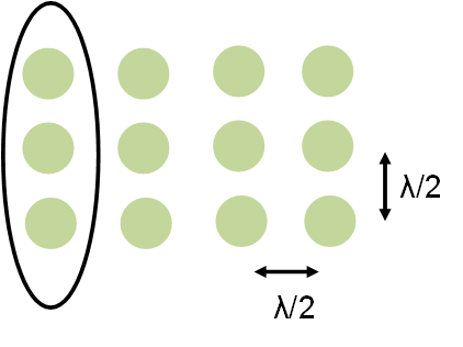
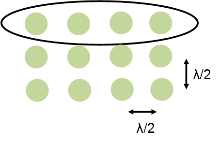
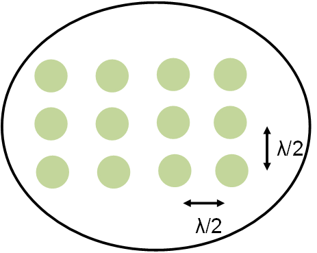
- Range-angle heat-map calculation – Two heat maps are computed: Range-Elevation-Angle and Range-Azimuth-Angle Heatmaps. A linear antenna array is formed at the azimuth plane to compute the azimuth angle spectrum for each range bin, and another linear antenna array is formed at elevation plane to compute the elevation angle spectrum. For example, in the ODS EVM board TDD MIMO configuration, the visual antenna array is shown in Figure 2-5. The Range-Elevation-Angle heat-map is computed using the 3-RX virtual horizontal antennae circled in Figure 2-5. The Range-Azimuth-Angle heat-map is computed using the 4-RX virtual horizontal antennae circled in Figure 2-6. A 3-RX signal can be formed as linear antenna array in elevation plane to compute range-elevation spectrum.
 Figure 2-5 Virtual Antenna Array for Range-Elevation-Angle Heat-Map Calculation
 Figure 2-6 Virtual Antenna Array for Range-Azimuth-Angle Heat-Map Calculation
The angle spectrum is computed using the covariance BF approach, as shown in Equation 1.
- Object Detection – The detection is done in the range-angle domain. Due to the limited angle resolution in our antenna pattern, object detection is limited to single target per range bin. In each range bin, a single peak is found which indicates the best angle in this range bin. Then, a CFAR window is formed to check whether this [range, angle] pair standout compare to its range neighbors. From range-azimuth heat-map and range elevation heat-map, two sets of peaks are found. Then configuration can choose to take the union or the interception of the two peak sets to form the final detection sets. The output is stored in the L2 memory
- Doppler estimation – For each detected point in range-angle space, Doppler is estimated using Doppler FFT. The output is stored in the L2 memory.
- Angle of arrival estimation – For each detected point, Doppler output for all the antenna is used to calculate the two-dimensional angle spectrum. Then the azimuth angle and elevation angle are then calculated from the single peak in the 2D angle spectrum. The output is stored in the L2 memory.
 Figure 2-7 Angle Spectrum