TIDUEZ8C december 2022 – june 2023
3.3 Software
Table 3-3 details the software flow.
Table 3-3 Software flow and
timing
| STEP | TIME (μs) | COMMENT |
|---|---|---|
| Board initialization | 2929 | One time after power up |
| Close SP + ADC Voltage settling | 500 | Time to close the switch SP and delay of 500 μs for the voltage at the ADC input to settle. Depending on capacitive loading this time needs to be adjusted (see Section 1.2). |
| Measure Viso,P and VDC,P | 126 | Both voltages are measured 20 times interleaved and averaged, to minimize noise |
| Open SP and close SN | 400 | A delay of 400 μs is implemented between the opening SP and closing SN. |
| ADC Voltage settling | 500 | Delay of 500 μs for the voltage at the ADC input to settle. Depending on capacitive loading this time needs to be adjusted (see Section 1.2). |
| Measure Viso,N and VDC,N | 126 | Both voltages are measured 20 times interleaved and averaged, to minimize noise |
| Calculate Riso,P and Riso,N | 13 | Final calculation of Riso,P and Riso,N |
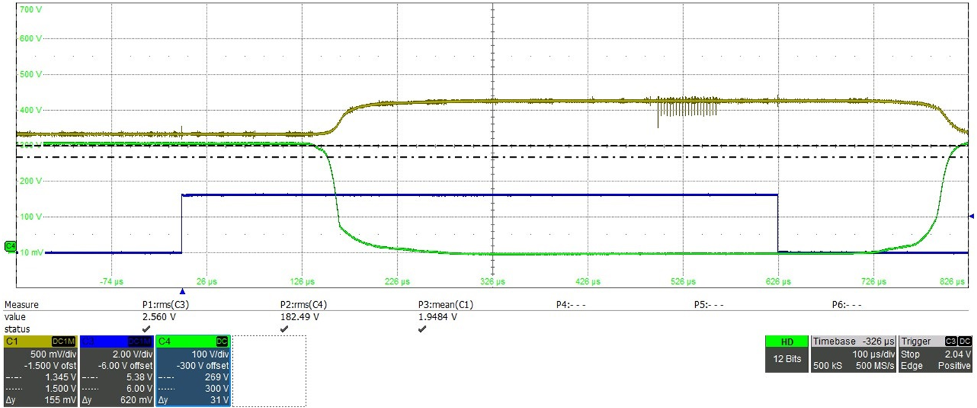
The software initialization takes about 3 ms and must be completed once after power up. Each measurement of the insulation resistances afterward takes 1.7 ms. This fast measurement time is one of the big advantages of using the TPSI2140 compared to a traditional relay for switching in the measurement path. The switching behavior of the TPIS2140 and voltage settling at the ADC input is shown in Figure 3-1.

Blue: Enable Signal, Green: Voltage
across TPSI2140, Yellow: Voltage at ADC input
Figure 3-1 Switching Behavior of TPSI2140
and ADC Input Voltage