TIDUF23 may   2023


  1.   Description
  2.   Resources
  3.   Features
  4.   Applications
  5.   5
  6. 1System Description
    1. 1.1 Key System Specifications
  7. 2System Overview
    1. 2.1 Block Diagram
    2. 2.2 Design Considerations
    3. 2.3 Highlighted Products
      1. 2.3.1  UCC5880-Q1
      2. 2.3.2  AM2634-Q1
      3. 2.3.3  TMS320F280039C-Q1
      4. 2.3.4  UCC14240-Q1
      5. 2.3.5  UCC12051-Q1
      6. 2.3.6  AMC3330-Q1
      7. 2.3.7  TCAN1462-Q1
      8. 2.3.8  ISO1042-Q1
      9. 2.3.9  ALM2403-Q1
      10. 2.3.10 LM5158-Q1
      11. 2.3.11 LM74202-Q1
    4. 2.4 System Design Theory
      1. 2.4.1 Microcontrollers
        1. 2.4.1.1 Microcontroller – C2000™
        2. 2.4.1.2 Microcontroller – Sitara™
      2. 2.4.2 Isolated Bias Supply
      3. 2.4.3 Power Tree
        1. 2.4.3.1 Introduction
        2. 2.4.3.2 Power Tree Block Diagram
        3. 2.4.3.3 12 V Distribution and Control
        4. 2.4.3.4 Gate Drive Supply
        5. 2.4.3.5 5-Volt Supply Domain
        6. 2.4.3.6 Current and Position Sensing Power
  8. 3Hardware, Software, Testing Requirements, and Test Results
    1. 3.1 Hardware Requirements
      1. 3.1.1 Hardware Board Overview
        1. 3.1.1.1 Control Board
        2. 3.1.1.2 MCU Control Card – Sitara™
        3. 3.1.1.3 MCU Control Card – C2000™
        4. 3.1.1.4 Gate Driver and Bias Supply Board
        5. 3.1.1.5 DC Bus Voltage Sense
        6. 3.1.1.6 SiC Power Module
          1. 3.1.1.6.1 XM3 SiC Power Module
          2. 3.1.1.6.2 Module Power Terminals
          3. 3.1.1.6.3 Module Signal Terminals
          4. 3.1.1.6.4 Integrated NTC Temperature Sensor
        7. 3.1.1.7 Laminated Busing and DC Bus Capacitors
          1. 3.1.1.7.1 Discharge PCB
    2. 3.2 Test Setup
      1. 3.2.1 Software Setup
        1. 3.2.1.1 Code Composer Studio Project
        2. 3.2.1.2 Software Structure
    3. 3.3 Test Procedure
      1. 3.3.1 Project Setup
      2. 3.3.2 Running the Application
    4. 3.4 Test Results
      1. 3.4.1 Isolated Bias Supply
      2. 3.4.2 Isolated Gate Driver
      3. 3.4.3 Inverter System
  9. 4General Texas Instruments High Voltage Evaluation (TI HV EVM) User Safety Guidelines
  10. 5Design and Documentation Support
    1. 5.1 Design Files
      1. 5.1.1 Schematics
      2. 5.1.2 BOM
      3. 5.1.3 PCB Layout Recommendations
        1. 5.1.3.1 Layout Prints
      4. 5.1.4 Altium Project
      5. 5.1.5 Gerber Files
      6. 5.1.6 Assembly Drawings
    2. 5.2 Tools and Software
    3. 5.3 Documentation Support
    4. 5.4 Support Resources
    5. 5.5 Trademarks
  11. 6Terminology
Module Power Terminals

The current loops in the XM3 power module have been designed such that they are wide, low profile, and evenly distributed between the devices so that they each have equivalent impedances across a switch position. The power terminals are vertically offset as shown in Figure 3-6 such that the bus bars between the DC link capacitors and the module can be laminated all the way up to the module without requiring bends, coining, standoffs, or complex isolation. A representative 3-phase inverter bussing is illustrated in Figure 3-7. Ultimately this achieves a low-inductance throughout the entire power loop from the DC link capacitors to the SiC devices. A XM3 module without devices was connected to a Keysight E4990A Impedance Analyzer to extract the parasitic inductance of the package. The power loop inductance from V+ to V- is 6.7 nH measured at 10 MHz.
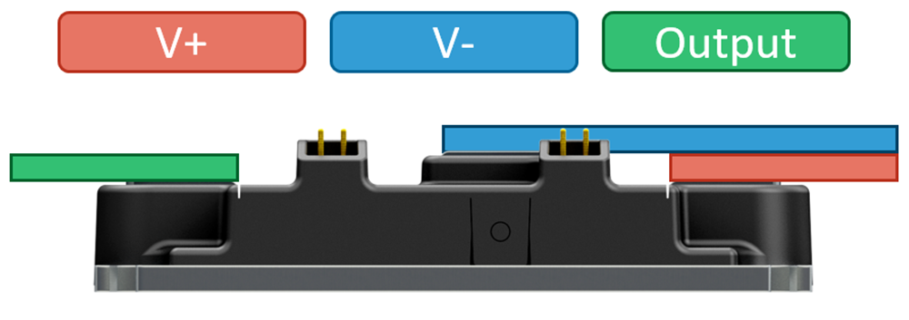
GUID-20230418-SS0I-0NWF-SDMR-DSVKKFJMGGLB-low.png Figure 3-6 Side View of XM3 Module Showing Non-planar Power Leads
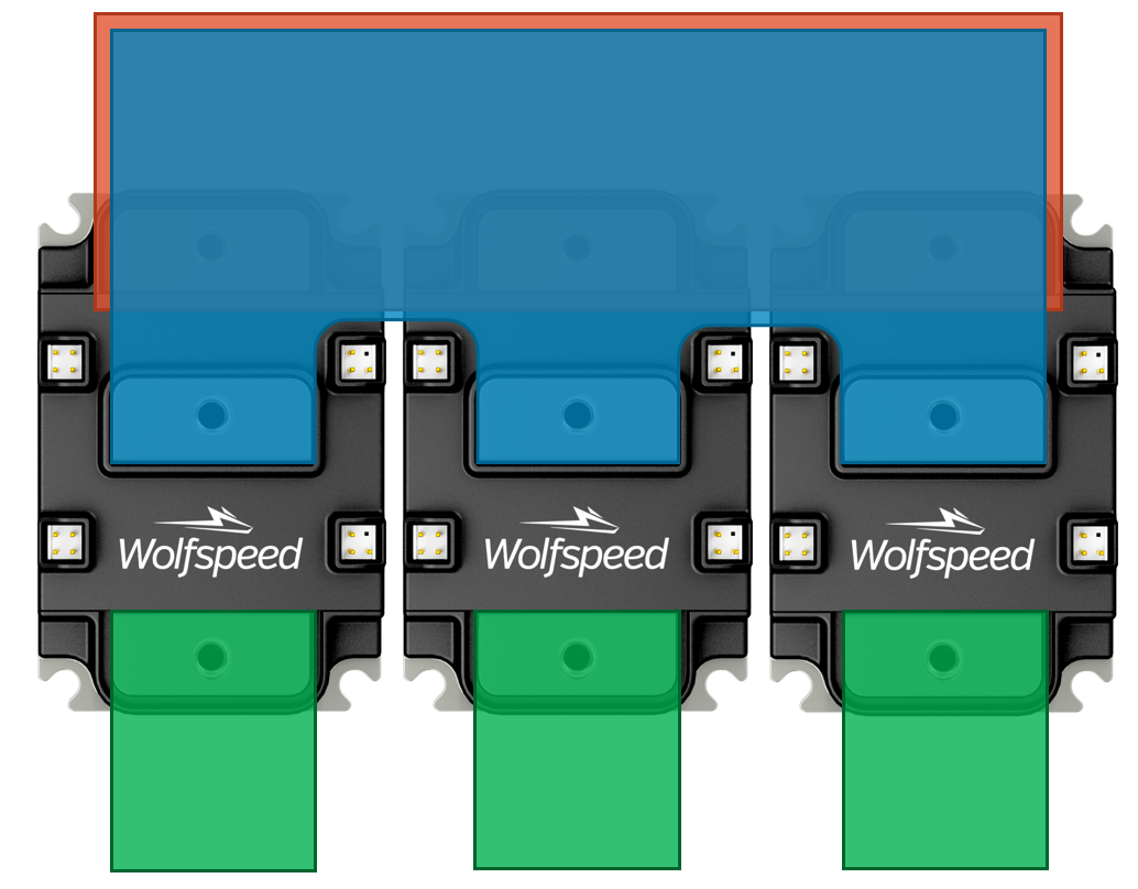
GUID-20230422-SS0I-2FFK-8FS6-J7FJNRXWZRCN-low.png Figure 3-7 Illustration Showing 3-Phase Bussing Layout