SBAA376A june 2019 – may 2023 ADS8578S , ADS8584S , ADS8586S , ADS8588H , ADS8588S , ADS8598H , ADS8598S , ADS8661 , ADS8664 , ADS8665 , ADS8668 , ADS8671 , ADS8674 , ADS8675 , ADS8678 , ADS8681 , ADS8684 , ADS8684A , ADS8685 , ADS8688 , ADS8688A , ADS8688AT , ADS8688W , ADS8689 , ADS8691 , ADS8694 , ADS8695 , ADS8698 , ADS8699
| Input | ADC Input | Digital Output ADS8588S |
|---|---|---|
| VinMax = +10 V | CH_nP = +10 V | 7FFFFH |
| VIN = 0 V | CH_nP = 0 V | 0000H |
| VinMin = –10 V | CH_nP = –10 V | 8000H |
| Power Supplies and Input | ||||
|---|---|---|---|---|
| AVDD | DVDD | Normal Input VIN |
Absolute Maximum Input Voltage Rating(Vin_Abs) | Absolute Maximum Input Current Rating(Iin_Abs) |
| +5 V | +3.3 V | ±10 V | ±15 V | ±10 mA |
Design Description
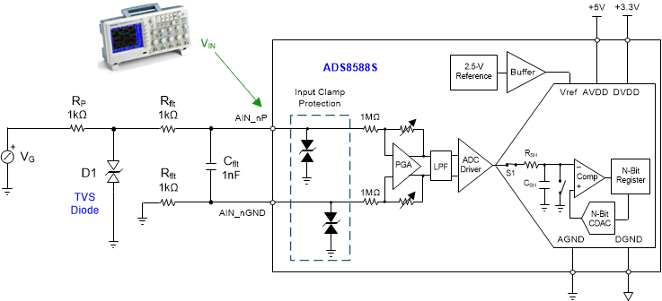
This circuit describes a solution to protect high-voltage SAR ADCs with integrated analog front end (AFE) from electrical overstress. The protection is implemented with an external transient voltage suppressor (TVS) diode, current-limiting resistors, and an RC filter. This document shows the impact that the external protection clamp has on system performance and introduces how to improve the performance. This circuit is useful in the following end equipment: Multifunction relays, AC analog input modules, and Train control and management systems. For protecting low-voltage SAR ADC from electrical overstress, see Circuit for protecting low-voltage SAR ADC from electrical overstress with minimal impact on performance.
Specifications
| Specification | Goal | Measured |
|---|---|---|
| Maximum continuous fault voltage | ±40 V | No damage with 40-V peak sinusoidal wave applied |
| SNR (ADS8588S) | 91.0 dB (±10-V range) | 92.0 dB |
| THD (ADS8588S) | –114 dB | –81.8 dB |
Design Notes
- The TVS diode is usually used as an electrical overstress protection for high-voltage SAR ADCs with integrated AFE because this kind of ADC only requires a single +5-V analog power supply but supports high-voltage analog input. For example, the ADS8588S device supports ±10 V on a 5-V analog supply. The TVS diode turns on and clamps the input voltage at its breakdown voltage.
- RP is used to limit the current into the TVS diode and the ADC, this resister is helpful to clamp the input fault signal with TVS diode together. The component selection in the external protection circuitry depends on the absolute maximum input voltage and current ratings on the particular ADC and the fault signal. See the component selection section for the details.
- Select a C0G type capacitor for Cfilt to minimize the distortion.
- See the Electrical Overstress on Data Converters video in the TI Precision Labs video series for a theoretical explanation of overstress on data converters. This series discusses the details on protection solutions for different types of ADCs including diode selection and current-limiting resistor selection.
Component Selection
- Select a bidirectional TVS diode
according to the following guidelines:
- VR ≥ VIN (VR is the standoff voltage of the TVS diode, VIN is the normal input voltage of the ADC that is ±10 V on the ADS8588S device)
- VBR ≤ Vin_Abs (VBR is the breakdown voltage of the TVS diode, Vin_Abs is the absolute input voltage ADC that is ±15 V on the ADS8588S device)
- Also, select a bidirectional TVS
diode according to the following restrictions:
- Low-leakage current, since the leakage current is translated into an offset voltage error when it flows through a series resistance.
- Low capacitance as the capacitance has a strong voltage coefficient and distorts the input signal.
- The TVS diode can dissipate the maximum power during fault condition. The steady-state power dissipation of the TVS diode should be higher than the maximum power from the fault signal.
Based on these guidelines, the PGSMAJ10CA bidirectional TVS diode from Taiwan Semiconductor Manufacturing Company, Ltd. ( TSMC®) is used in this design to protect the ADS8588S device which is a widely-used TVS diode. The specifications for three different TVS diodes are given later in this document to compare all the pertinent parameters.
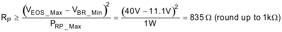
- The following equation finds a
minimum value of RP to limit its power dissipation to a specified
level during a fault condition. The equation uses the maximum fault voltage
(VEOS_Max), the minimum breakdown voltage (VBR_Min),
and the maximum power dissipation (PRP_Max). In this design, the
maximum electrical overstress signal was selected to be ±40 V because this is a
common requirement for industrial systems. The minimum breakdown voltage of the
PGSMAJ10CA diode is 11.1 V, and the maximum resistor power is set to 1 W. In
this example, the minimum value of RP is 835 Ω, and RP is
rounded up to 1 kΩ. It is important to note that the resistor power rating must
have margin to operate safely over temperature. A typical guideline is to double
the power rating (2 W, in this example).
The following equation shows the maximum current in RP during an electrical overstress fault event:
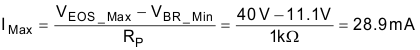
Using the maximum current (IMax) and maximum clamping voltage (VC_Max) on the PGSMAJ10CA TVS diode, calculate the maximum power dissipated on the diode during an electrical overstress fault event. The objective of this equation is to make sure that the correct power rating of TVS diode is used. For the PGSMAJ10CA diode, the steady-state power rating is 1W. Thus, there is margin in this design as we do not expect more then 491mW of continuous power.

- The resistor Rflt acts
as a filter with the capacitor Cflt and also to limit the current to
the ADC input under a fault condition. The absolute maximum input voltage
(Vin_Abs) of the ADS8588S device is ±15V and the maximum input
current (Iin_Abs) is ±10mA. The PGSMAJ10CA TVS diode has 17-V maximum
clamping voltage (VC_Max) when 23.5-A peak current (IPP)
are flowing it for a brief period of time. Hence, the minimum value of
Rflt can be determined by:
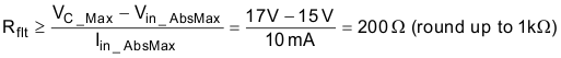
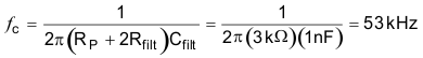
The equation calculated Rfilt to be 200Ω. In this design, the 200Ω is rounded up to 1kΩ to add significant design margin. Rfilt can be adjusted to set the cutoff frequency of the filter as step 5 shows.
- The capacitor Cflt in parallel with Rflt is used to filter the noise from the front-end circuit. The equation for the cutoff frequency based on the input resistors and capacitors follows. The exact value may not be critical, so a standard value of 1nF is used in this design.
ADC Input (AIN_P) Overvoltage Condition
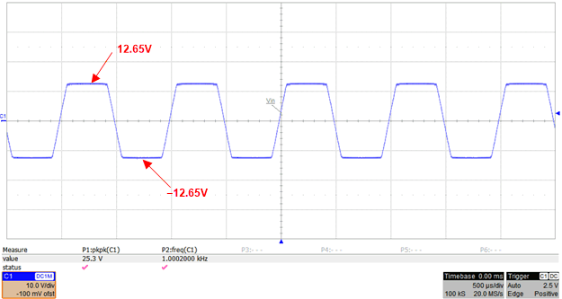
The following figure shows the ADC input voltage when a high-voltage continuous overvoltage sinusoidal wave signal (60 Vpp) is applied. Note that the external bidirectional TVS diode is turned on and the overvoltage sinusoidal wave signal has been clamped to ±12.5Vpeak, which is less than ±15-V absolute maximum input voltage (Vin_Abs) on the ADS8588S device, so the ADC device is protected from the overvoltage signal.
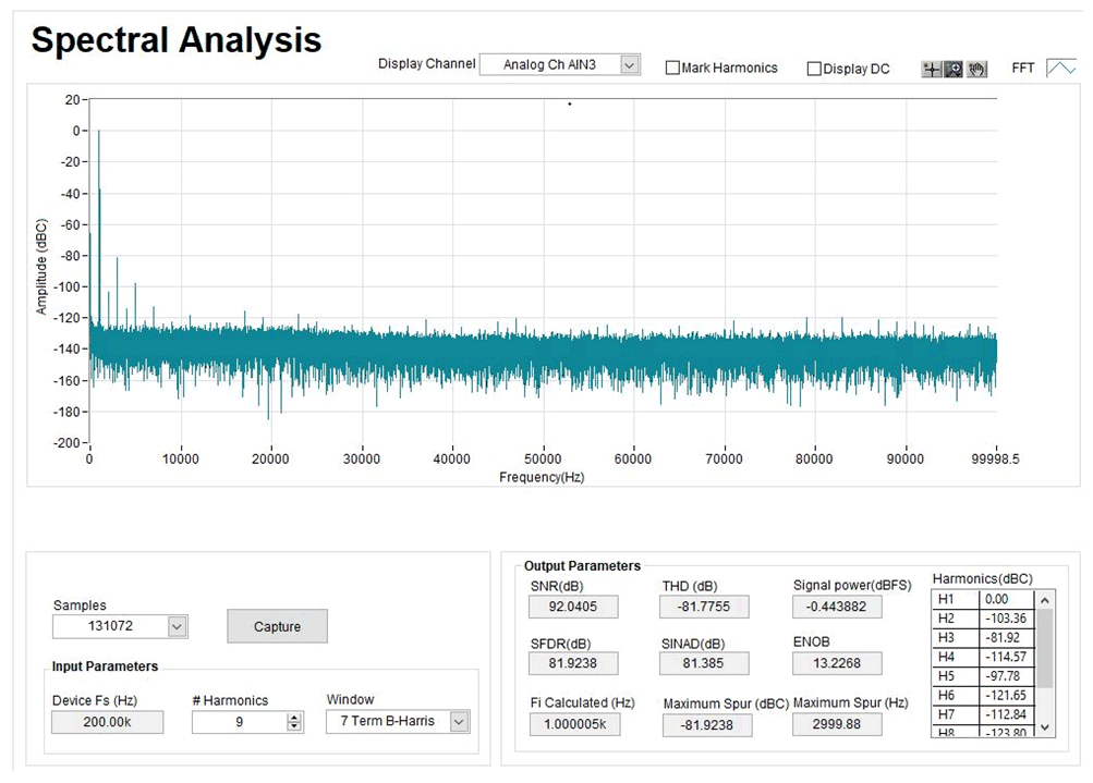
AC (SNR and THD) Performance Checked on Hardware
The following spectral analysis is measured using the ADS8588SEVM-PDK and overvoltage protection (OVP) board specifically designed for this test. The measured THD performance with all the protection circuitry including the TVS diode is worse than the typical specification in the ADS8588S 16-Bit, High-Speed, 8-Channel, Simultaneous-Sampling ADC With Bipolar Inputs on a Single Supply Data Sheet (measured SNR = 92dB,THD = –81.8dB).
Capacitance Variation on TVS Diode Causes Worse THD
The previous test result shows that the measured SNR performance meets the specification in the ADS8588S data sheet; however, the measured THD performance is worse than the specification in the data sheet. The key reason to cause the worse THD performance is the large capacitance variation which is changed with the voltage applied on the TVS diode, see the Electrical Overstress (EOS) and Electrostatic Discharge (ESD) on Analog-to-Digital Converters (ADC) video (part of the TI Precision Labs video series) for detailed theory and analysis on this subject.
There are two solutions to improve the system THD performance: use a low-capacitance variation bidirectional TVS diode, reduce input signal frequency with less impact from the capacitance and variation on the TVS diode, if this is acceptable in the system.
Low Capacitance Variation TVS Diode
The capacitance of the TVS diode has a strong impact on distortion, and the following table compares the measured results for TVS diodes with different capacitance specifications. This table shows improved THD performance with decreasing capacitance on the TVS diodes. The low-capacitance bidirectional TVS diode, PGSMAJ10CA, from TSMC shows a better THD performance (–81.8dB) with the same protection circuitry. To achieve a better THD performance, use the TVS diode with further lower capacitance and variation.
| Part Numbers | Reverse Standoff Voltage (VR) |
Breakdown Voltage (VBR) |
Clamping Voltage MAX (VC) |
Capacitance Variation (CT) |
Reverse Leakage MAX (IR at VR) |
Peak Pulse Current (IPP) | Measured THD (dB) | Clamped Voltage (1kΩ Rp, VIN = 40 V) |
|
|---|---|---|---|---|---|---|---|---|---|
| MIN | MAX | ||||||||
| SMCJ10CA | 10 V | 11.1 | 12.3 | 17V | 2.3nF to 10nF | 5µA | 88.3A | –69.6 | ±12.6V |
| SMA6J10A | 10 V | 11.1 | 12.3 | 15.7V | 200 to 400pF | 5µA | 38.2A | –79.5 | ±12.6V |
| PGSMAJ10CA | 10 V | 11.1 | 12.3 | 17V | 80 to 160pF | 5µA | 23.5A | –81.8 | ±12.6V |
| CDSOD323-T12C (1) | 12V | 13.3 | 19V | 3pF | 1µA | 11A | –102.1 | ±15.6V | |
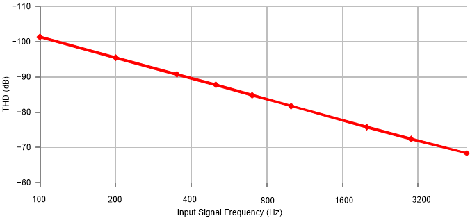
Lower Input Signal Frequency
The following figure shows that the measured THD performance is improved by reducing input signal frequency. This graph was measured with the PGSMAJ10CA TVS diode, RP = 1kΩ, Rflt = 1kΩ, Cflt = 1nF and ADS8588S at 200kSPS on the EVM.
Design Featured Devices and Alternative Parts
| Device | Key Features | Link | Other Possible Devices |
|---|---|---|---|
| ADS8588S | 16-bit, 200-kSPS, 8-channel simultaneous-sampling, single-supply bipolar-input SAR ADC | http://www.ti.com/product/ADS8588S | http://www.ti.com/adcs |
| ADS8688 | 16-bit, 500-kSPS, 8-channel non-simultaneous-sampling, single-supply with bipolar-input SAR ADC | http://www.ti.com/product/ADS8688 | http://www.ti.com/adcs |
| ADS8681 | 16-bit, 1-MSPS, single-channel, single-supply with bipolar-input SAR ADC | http://www.ti.com/product/ADS8681 | http://www.ti.com/adcs |
Design References
See Analog Engineer's Circuit Cookbooks for TI's comprehensive circuit library.