SNAS393D March 2007 – November 2016 LME49720
PRODUCTION DATA.
- 1 Features
- 2 Applications
- 3 Description
- 4 Revision History
- 5 Device Comparison Table
- 6 Pin Configuration and Functions
- 7 Specifications
- 8 Parameter Measurement Information
- 9 Detailed Description
- 10Application and Implementation
- 11Power Supply Recommendations
- 12Layout
- 13Device and Documentation Support
- 14Mechanical, Packaging, and Orderable Information
Package Options
Mechanical Data (Package|Pins)
Thermal pad, mechanical data (Package|Pins)
Orderable Information
1 Features
- Easily Drives 600Ω Loads
- Optimized for Superior Audio Signal Fidelity
- Output Short Circuit Protection
- PSRR and CMRR Exceed 120dB (typ)
- SOIC, PDIP, TO-99 Metal Can Packages
- Key Specifications
- Power Supply Voltage Range: ±2.5 to ±17V
- THD+N (AV = 1, VOUT = 3VRMS, fIN = 1kHz):
- RL = 2kΩ: 0.00003% (typ)
- RL = 600Ω: 0.00003% (typ)
- Input Noise Density: 2.7nV/√Hz (typ)
- Slew Rate: ±20V/μs (typ)
- Gain Bandwidth Product: 55MHz (typ)
- Open Loop Gain (RL = 600Ω): 140dB (typ)
- Input Bias Current: 10nA (typ)
- Input Offset Voltage: 0.1mV (typ)
- DC Gain Linearity Error: 0.000009%
2 Applications
- Ultra High Quality Audio Amplification
- High Fidelity Preamplifiers
- High Fidelity Multimedia
- State of the Art Phono Pre Amps
- High Performance Professional Audio
- High Fidelity Equalization and Crossover Networks
- High Performance Line Drivers
- High Performance Line Receivers
- High Fidelity Active Filters
3 Description
The LME49720 device is part of the ultra-low distortion, low noise, high slew rate operational amplifier series optimized and fully specified for high performance, high fidelity applications. Combining advanced leading-edge process technology with state-of-the-art circuit design, the LME49720 audio operational amplifiers deliver superior audio signal amplification for outstanding audio performance. The LME49720 combines extremely low voltage noise density (2.7nV/√Hz) with vanishingly low THD+N (0.00003%) to easily satisfy the most demanding audio applications.
Device Information(1)
| PART NUMBER | PACKAGE | BODY SIZE (NOM) |
|---|---|---|
| LME49720 | TO-99 (8) | 9.08mm × 9.08mm |
| SOIC (8) | 4.90mm × 3.91mm | |
| PDIP (8) | 9.81mm × 6.35mm |
- For all available packages, see the orderable addendum at the end of the data sheet.
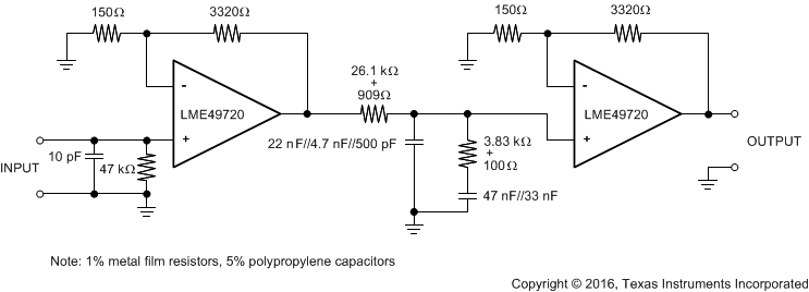
Passively Equalized RIAA Phono Preamplifier
