SLVSAA2D March 2010 – January 2016 TPS65182 , TPS65182B
PRODUCTION DATA.
- 1 Features
- 2 Applications
- 3 Description
- 4 Revision History
- 5 Pin Configuration and Functions
- 6 Specifications
-
7 Detailed Description
- 7.1 Overview
- 7.2 Functional Block Diagram
- 7.3
Feature Description
- 7.3.1 Modes of Operation
- 7.3.2 Mode Transistions
- 7.3.3 Wake-Up and Power Up Sequencing
- 7.3.4 Dependencies Between Rails
- 7.3.5 Soft-Start
- 7.3.6 VCOM Adjustment
- 7.3.7 VPOS and VNEG Supply Tracking
- 7.3.8 Fault Handling and Recovery
- 7.3.9 Power Good Pin
- 7.3.10 Panel Temperature Monitoring
- 7.3.11 NTC Bias Circuit
- 7.4 Device Functional Modes
- 7.5 Register Maps
- 8 Application and Implementation
- 9 Power Supply Recommendations
- 10Layout
- 11Device and Documentation Support
- 12Mechanical, Packaging, and Orderable Information
Package Options
Mechanical Data (Package|Pins)
- RGZ|48
Thermal pad, mechanical data (Package|Pins)
- RGZ|48
Orderable Information
1 Features
- Single Chip Power Management Solution for
E Ink® Vizplex™ Electronic Paper Displays - Generates Positive and Negative Gate and Source Driver Voltages and Back-Plane Bias from a Single, Low-Voltage Input Supply
- 3-V to 6-V Input Voltage Range
- Boost Converter for Positive Rail Base
- Inverting Buck-Boost Converter for Negative Rail Base
- Two Adjustable LDOs for Source Driver Supply
- LDO1: 15 V, 120 mA (VPOS)
- LDO2: –15 V, 120 mA (VNEG)
- Accurate Output Voltage Tracking
- VPOS - VNEG = ±50 mV
- Two Charge Pumps for Gate Driver Supply
- CP1: 22 V, 10 mA (VDDH)
- CP2: –20 V, 12 mA, (VEE)
- Adjustable VCOM Driver for Accurate Panel-Backplane Biasing
- –0.3 V to –2.5 V
- Adjustable Through External Potentiometer
- 15-mA Max Integrated Switch
- Thermistor Monitoring
- –10°C to 85°C Temperature Range
- ±1°C Accuracy from 0°C to 50°C
- I2C Serial Interface
- Slave Address 0x48h (1001000)
- Flexible Power-Up Sequencing
- Sleep Mode Support
- Thermally Enhanced Package for Efficient Heat Management
(48-Pin 7 mm × 7 mm × 0.9 mm VQFN)
2 Applications
- Power Supply for Active Matrix E Ink Vizplex Panels
- E-Book Readers
- EPSON® S1D13522 (ISIS) Timing Controller
- EPSON S1D13521 (Broadsheet) Timing Controller
- Application Processors With Integrated or Software Timing Controller (OMAP™)
3 Description
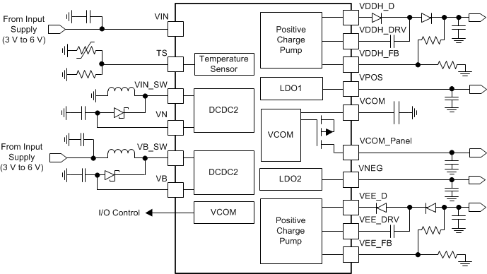
The TPS65182x device is a single-chip power supplies designed to for E Ink Vizplex displays used in portable e-reader applications and support panel sizes up to 9.7 inches. Two high efficiency DC/DC boost converters generate ±17-V rails which are boosted to 22 V and –20 V by two change pumps to provide the gate driver supply for the Vizplex panel.
Device Information(1)
| PART NUMBER | PACKAGE | BODY SIZE (NOM) |
|---|---|---|
| TPS65182(2) | VQFN (48) | 7.00 mm × 7.00 mm |
| TPS65182B |
- For all available packages, see the orderable addendum at the end of the data sheet.
- Not recommended for new design.
Typical Application Schematic
