Packaging information
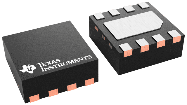
| Package | Pins WSON (DSG) | 8 |
| Operating temperature range (°C) -40 to 125 |
| Package qty | Carrier 250 | SMALL T&R |
Features for the OPA855
- High gain bandwidth product: 8GHz
- Decompensated, gain ≥ 7V/V (stable)
- Low input voltage noise: 0.98nV/√Hz
- Slew rate: 2750V/µs
- Low
Input capacitance:
- Common-mode: 0.6pF
- Differential: 0.2pF
- Wide input common-mode range:
- 0.4V from positive supply
- 1.1V from negative supply
- 3VPP total output swing
- Supply voltage range: 3.3V to 5.25V
- Quiescent current: 17.8mA
- Package: 8-pin WSON
- Bare die
- Temperature range: –40°C to +125°C
Description for the OPA855
The OPA855 is a wideband, low-noise operational amplifier with bipolar inputs for wideband transimpedance and voltage amplifier applications. When the device is configured as a transimpedance amplifier (TIA), the 8GHz gain bandwidth product (GBWP) enables high closed-loop bandwidths at transimpedance gains of up to tens of kilohms.
The following graph shows the bandwidth and noise performance of the OPA855 as a function of the photodiode capacitance when the amplifier is configured as a TIA. The total noise is calculated along a bandwidth range extending from dc to the calculated frequency (f) on the left scale. The OPA855 package has a feedback pin (FB) that simplifies the feedback network connection between the input and the output.
The OPA855 is optimized to operate in optical time-of-flight (ToF) systems where the OPA855 is used with time-to-digital converters, such as the TDC7201. Use the OPA855 to drive a high-speed analog-to-digital converter (ADC) in high-resolution LIDAR systems with a differential output amplifier, such as the THS4541 or LMH5401 devices.