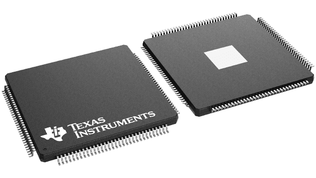
128-pin (NNB) package image

ADC081500CIYB/NOPB アクティブ

8 ビット、1.5GSPS、A/D コンバータ (ADC)

価格

数量 価格
+

品質に関する情報

定格 Catalog
RoHS はい
REACH はい
リード端子の仕上げ / ボールの原材料 SN
MSL rating / リフローピーク温度 Level-3-260C-168 HR
品質、信頼性
、パッケージングの情報

記載されている情報:

  • RoHS
  • REACH
  • デバイスのマーキング
  • リード端子の仕上げ / ボールの原材料
  • MSL rating / リフローピーク温度
  • MTBF/FIT 推定値
  • 使用原材料
  • 認定試験結果
  • 継続的な信頼性モニタ試験結果
表示またはダウンロード
製造に関する追加情報

記載されている情報:

  • ファブ拠点
  • アセンブリ拠点
表示

輸出分類

*参考用

  • US ECCN (米国輸出規制分類番号):3A001A5A1

パッケージ情報

パッケージ | ピン数 HLQFP (NNB) | 128
動作温度範囲 (℃) -40 to 85
パッケージ数量 | キャリア 60 | JEDEC TRAY (10+1)

ADC081500 の特徴

  • Internal Sample-and-Hold
  • Single +1.9V ±0.1V Operation
  • Choice of SDR or DDR output clocking
  • Multiple ADC Synchronization Capability
  • Guaranteed No Missing Codes
  • Serial Interface for Extended Control
  • Fine Adjustment of Input Full-Scale Range and Offset
  • Duty Cycle Corrected Sample Clock

  • Key Specifications

    Resolution

    8 Bits

    Max Conversion Rate

    1.5 GSPS (min)

    Bit Error Rate

    10 -18 (typ)

    ENOB @ 748 MHz Input

    7.3 Bits (typ)

    DNL

    ±0.15 LSB (typ)

    Power Consumption

    Operating

    1.2 W (typ)

    Power Down Mode

    3.5 mW (typ)


    ADC081500 に関する概要

    The ADC081500 is a low power, high performance CMOS analog-to-digital converter that digitizes signals to 8 bits resolution at sample rates up to 1.7 GSPS. Consuming a typical 1.2 W at 1.5 GSPS from a single 1.9 Volt supply, this device is guaranteed to have no missing codes over the full operating temperature range. The unique folding and interpolating architecture, the fully differential comparator design, the innovative design of the internal sample-and-hold amplifier and the self-calibration scheme enable a very flat response of all dynamic parameters beyond Nyquist, producing a high 7.3 ENOB with a 748 MHz input signal and a 1.5 GHz sample rate while providing a 10 -18 B.E.R. Output formatting is offset binary and the LVDS digital outputs are compatible with IEEE 1596.3-1996, with the exception of an adjustable output offset voltage between 0.8V and 1.2V.

    The converter output has a 1:2 demultiplexer that feeds two LVDS buses and reduces the output data rate on each bus to one-half the sample rate.

    The converter typically consumes less than 3.5 mW in the Power Down Mode and is available in a 128-lead, thermally enhanced exposed pad LQFP and operates over the Industrial (-40°C TA +85°C) temperature range.

    価格

    数量 価格
    +

    キャリア オプション

    パーツの数量に応じて、リール全体、カスタム リール、カット テープ、チューブ、トレイを含め、さまざまなキャリア オプションを選択できます。

    カスタム リールとは、ご注文の数量に正確に一致するように 1 本のリールからカットした一定の長さのテープのことであり、ロット コードと日付コードのトレーサビリティを維持できます。業界標準に従い、真鍮製のスペーサーを使用し、カット済みテープの両側に 1 本の 18 インチ (45cm) フラット リーダー (先行) テープと、1 本の 18 インチ (45cm) フラット トレーラ (後続) テープを取り付けた状態であり、自動アセンブリ マシンに直接供給することができます。カスタム リールをご注文になった場合、リール処理料金がかかります。

    カット テープとは、リールから切り離した一定の長さのテープのことです。ご注文の数量にするために、納品時に複数のカット テープまたは複数の箱に分割されることがあります。

    在庫状況により、多くの場合、チューブトレイ梱包デバイスは、箱、またはチューブやトレイに梱包された形態で出荷されます。すべてのテープ、チューブ、またはサンプル ボックスは、TI 社内の静電気放電 (ESD) 保護と湿度感度レベル (MSL) 保護の要件に従って梱包してあります。

    詳細はこちら

    ロットと日付コードの選択が可能な場合があります。

    カートにご希望の数量を追加し、チェックアウト プロセスを開始すると、既存の在庫からロットまたは日付コードを選択できる各種オプションが表示されます。

    詳細はこちら