パッケージ情報
| パッケージ | ピン数 CFP (HFG) | 84 |
| 動作温度範囲 (℃) -55 to 125 |
| パッケージ数量 | キャリア 1 | OTHER |
ADS5444-SP の特徴
- 13 Bit Resolution
- 250 MSPS Sample Rate
- SNR = 67.6 dBc at 230 MHz IF and 250 MSPS
- SFDR = 74.0 dBc at 230 MHz IF and 250 MSPS
- 2.2 VPP Differential Input Voltage
- Fully Buffered Analog Inputs
- 5 V Analog Supply Voltage
- LVDS Compatible Outputs
- Total Power Dissipation: 2 W
- Offset Binary Output Format
- Pin Compatible With the ADS5440
- Military Temperature Range
(–55°C to 125°C Tcase)
ADS5444-SP に関する概要
The ADS5444 is a 13 bit 250 MSPS analog-to-digital converter (ADC) that operates from a 5 V supply, while providing LVDS-compatible digital outputs from a 3.3 V supply. The ADS5444 input buffer isolates the internal switching of the onboard track and hold (T&H) from disturbing the signal source. An internal reference generator is also provided to further simplify the system design. The ADS5444 has outstanding low noise and linearity over input frequency.
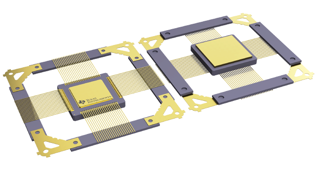
The ADS5444 is available in a 84 pin ceramic nonconductive tie-bar package (HFG). The ADS5444 is built on a state-of-the-art Texas Instruments complementary bipolar process (BiCom3X) and is specified over the full military temperature range (–55°C to 125°C Tcase).
This CQFP package has built in vias that electrically and thermally connect the bottom of the die to a pad on the bottom of the package. To efficiently remove heat and provide a low-impedance ground path, a thermal land is required on the surface of the PCB directly underneath the body of the package. During normal surface mount flow solder operations, the heat pad on the underside of the package is soldered to this thermal land creating an efficient thermal path. Normally, the PCB thermal land has a number of thermal vias within it that provide a thermal path to internal copper areas (or to the opposite side of the PCB) that provide for more efficient heat removal. TI typically recommends an 11,9-mm2 board-mount thermal pad. This allows maximum area for thermal dissipation, while keeping leads away from the pad area to prevent solder bridging. A sufficient quantity of thermal/electrical vias must be included to keep the device within recommended operating conditions. This pad must be electrically at ground potential.