パッケージ情報
| パッケージ | ピン数 VQFN (RHA) | 40 |
| 動作温度範囲 (℃) -40 to 85 |
| パッケージ数量 | キャリア 250 | SMALL T&R |
ADS61JB46 の特徴
- Output Interface:
- Single-Lane and Dual-Lane Interfaces
- Maximum Data Rate: 3.125 Gbps
- Meets JEDEC JESD204A Specification
- CML Outputs with Current Programmable from 2 mA to 32 mA
- Power Dissipation:
- 583 mW at 160 MSPS in Dual-Lane Mode
- Power Scales Down with Clock Rate
- Input Interface: Buffered Analog Inputs
- SNR at 185-MHz IF: –72.7 dBFS
- Analog Input Dynamic Range: 2 VPP
- Reference Support:
External and Internal (Trimmed) - Supply:
- Analog and Digital: 1.8 V
- Input Buffer: 3.3 V
- Programmable Digital Gain: 0 dB to 6 dB
- Output: Straight Offset Binary or
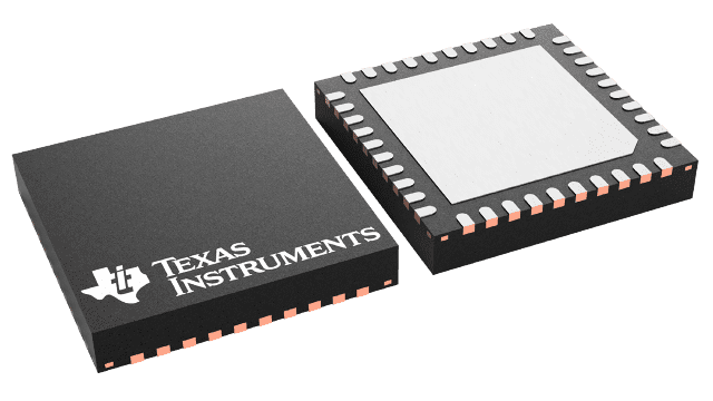
Twos Complement - Package: 6-mm × 6-mm QFN-40
ADS61JB46 に関する概要
The ADS61JB46 is a high-performance, low-power, single-channel, analog-to-digital converter with an integrated JESD204A output interface. Available in a 6-mm × 6-mm QFN package, with both single-lane and dual-lane output modes, the device offers an unprecedented level of compactness. The output interface is compatible to the JESD204A standard, with an additional mode (as per the IEEE standard 802.3-2002 part 3, clause 36.2.4.12) to interface seamlessly to the TI TLK family of SERDES transceivers. Equally impressive is the inclusion of an on-chip analog input buffer, providing isolation between the sample-and-hold switches and higher and more consistent input impedance.
The device is specified over the industrial temperature range (–40°C to +85°C).