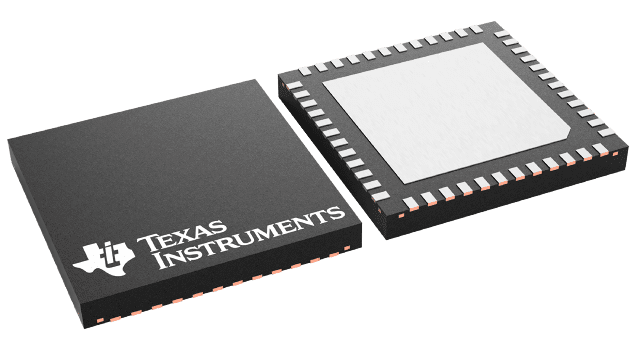
パッケージ情報
| パッケージ | ピン数 WQFN (RHS) | 48 |
| 動作温度範囲 (℃) -40 to 85 |
| パッケージ数量 | キャリア 2,500 | LARGE T&R |
LMK04101 の特徴
- Cascaded PLLatinum PLL Architecture
- PLL1Redundant Reference Inputs Loss of Signal
DetectionAutomatic and Manual Selection of
Reference Clock Input - PLL2Phase Detector Rate up to 100 MHzInput
Frequency-DoublerIntegrated VCO
- PLL1Redundant Reference Inputs Loss of Signal
- Outputs
- LVPECL/2VPECL, LVDS, and
LVCMOS Formats - Support Clock Rates up to 1080 MHz
- Five Dedicated Channel Divider Blocks
- Common Output Frequencies Supported:
30.72 MHz, 61.44 MHz, 62.5 MHz,
74.25 MHz, 75 MHz, 77.76 MHz, 100 MHz,
106.25 MHz, 125 MHz, 122.88 MHz,
150 MHz, 155.52 MHz, 156.25 MHz, 159.375 MHz,
187.5 MHz, 200 MHz,
212.5 MHz, 245.76 MHz, 250 MHz, 311.04 MHz,
312.5 MHz, 368.64 MHz,
491.52 MHz, 622.08 MHz, 625 MHz, 983.04 MHz
- LVPECL/2VPECL, LVDS, and
- MICROWIRE (SPI) Programming Interface
- Industrial Temperature Range: –40 to 85 °C
- 3.15 V to 3.45 V Operation
- Package: 48 Pin WQFN (7.0 × 7.0 × 0.8 mm)
LMK04101 に関する概要
The LMK04100 family of precision clock conditioners provides jitter cleaning, clock multiplication and distribution without the need for high-performance VCXO modules.
When connected to a recovered system reference clock and a VCXO, the device generates 5 low jitter clocks in LVCMOS, LVDS, or LVPECL formats.
