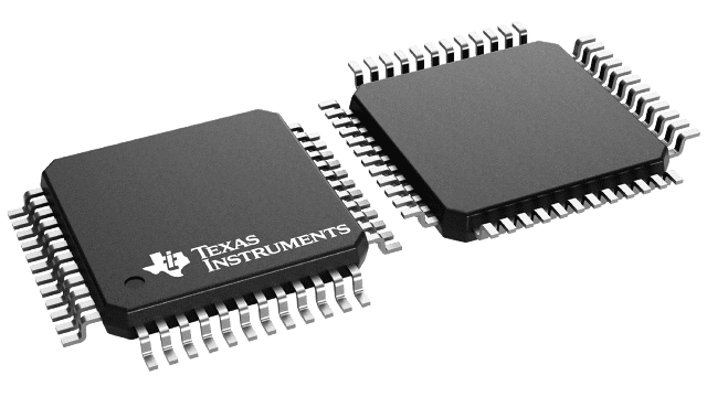
パッケージ情報
| パッケージ | ピン数 TQFP (PFB) | 48 |
| 動作温度範囲 (℃) -40 to 85 |
| パッケージ数量 | キャリア 250 | JEDEC TRAY (10+1) |
THS0842 の特徴
- Dual Simultaneous Sample and Hold Inputs
- Differential or Single-Ended Analog Inputs
- 8-Bit Resolution 40 MSPS Sampling Analog-to-Digital Converter (ADC)
- Single or Dual Parallel Bus Output
- Low Power Consumption: 275 mW Typ Using External References
- Wide Analog Input Bandwidth: 600 MHz Typ
- 3.3 V Single-Supply Operation
- 3.3 V TTL/CMOS-Compatible Digital I/O
- Internal or External Bottom and Top Reference Voltages
- Adjustable Reference Input Range
- Power-Down (Standby) Mode
- 48-Pin Thin Quad Flat Pack (TQFP) Package
- Applications
- Digital Communications (Baseband Sampling)
- Cable Modems
- Set Top Boxes
- Test Instruments
THS0842 に関する概要
The THS0842 is a dual 8-bit 40 MSPS high-speed A/D converter. It alternately converts each analog input signal into 8-bit binary-coded digital words up to a maximum sampling rate of 40 MSPS with an 80 MHz clock. All digital inputs and outputs are 3.3 V TTL/CMOS-compatible.
Thanks to an innovative single-pipeline architecture implemented in a CMOS process and the 3.3 V supply, the device consumes very little power. In order to provide maximum flexibility, both bottom and top voltage references can be set from user supplied voltages. Alternately, if no external references are available, on-chip references can be used which are also made available externally. The full-scale range is 1 Vpp, depending on the analog supply voltage. If external references are available, the internal references can be powered down independently from the rest of the chip, resulting in an even greater power saving.
The device is specifically suited for the baseband sampling of wireless local loop (WLL) communication, cable modems, set top boxes (STBs), and test instruments.
