패키징 정보
| 패키지 | 핀 VQFN (RGC) | 64 |
| 작동 온도 범위(°C) -40 to 85 |
| 패키지 수량 | 캐리어 250 | SMALL T&R |
DAC5681Z의 주요 특징
- 16-Bit Digital-to-Analog Converter (DAC)
- 1.0 GSPS Update Rate
- 16-Bit Wideband Input LVDS Data Bus
- 8 Sample Input FIFO
- High Performance
- 73-dBc ACLR WCDMA TM1 at 180 MHz
- 2x to 32x Clock Multiplying PLL/VCO
- 2x or 4x Interpolation Filters
- Stopband Transition 0.4–0.6 Fdata
- Filters Configurable in Either Low-Pass or
High-Pass Mode- Allows Selection of Higher Order Image
- On-Chip 1.2-V Reference
- 2 to 20-mA Differential Scalable Output
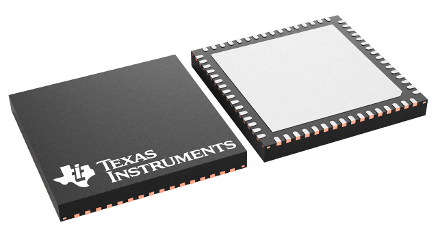
- 64-Pin 9-mm × 9-mm VQFN Package
- APPLICATIONS
- Cellular Base Stations
- Broadband Wireless Access (BWA)
- WiMAX 802.16
- Fixed Wireless Backhaul
- Cable Modem Termination System (CMTS)
All other trademarks are the property of their respective owners
DAC5681Z에 대한 설명
The DAC5681Z is a 16-bit 1.0 GSPS digital-to-analog converter (DAC) with wideband LVDS data input, integrated 2x to 4x interpolation filters, on-board clock multiplier, and internal voltage reference. The DAC5681Z offers superior linearity, noise, crosstalk, and PLL phase noise performance.
The DAC5681Z integrates a wideband LVDS port with on-chip termination. Full-rate input data can be transferred to a single DAC channel, or half-rate and 1/4-rate input data can be interpolated by on-board 2x or 4x FIR filters. Each interpolation FIR is configurable in either low-pass or high-pass mode, allowing selection of a higher order output spectral image. An on-chip delay lock loop (DLL) simplifies LVDS interfacing by providing skew control for the LVDS input data clock.
The DAC5681Z is characterized for operation over the industrial temperature range of –40°C to 85°C and is available in a 64-pin VQFN package. Other members of the family include the dual-channel, interpolating DAC5682Z and the single-channel, non-interpolating DAC5681.