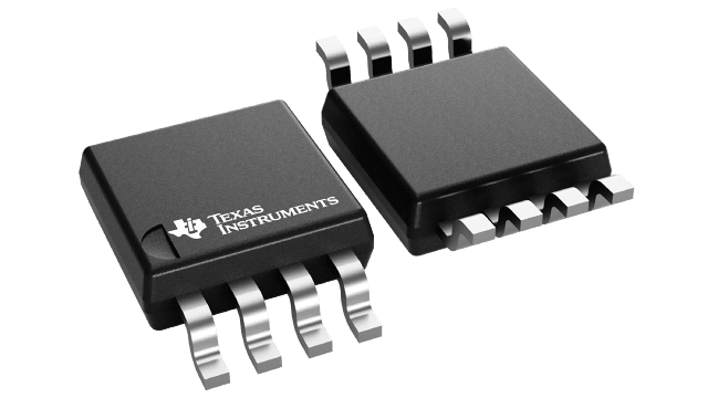
패키징 정보
| 패키지 | 핀 VSSOP (DGK) | 8 |
| 작동 온도 범위(°C) -40 to 105 |
| 패키지 수량 | 캐리어 2,500 | LARGE T&R |
TPS22958의 주요 특징
- Integrated N-Channel Load Switch
- Input Voltage Range: 0.6 V to 5.5 V
- VBIAS Voltage Range: 2.5 V to 5.5 V
- RON Resistance
- RON = 14 mΩ at VIN = 5 V (VBIAS = 5 V)
- RON = 13 mΩ at VIN = 3.3 V (VBIAS = 5 V)
- RON = 13 mΩ at VIN = 1.8 V (VBIAS = 5 V)
- 4 A Maximum Continuous Switch Current (DGK Package)
- 6 A Maximum Continuous Switch Current (DGN Package)
- Low Quiescent Current
- 55 µA at VBIAS = 5 V
- Low Control Input Threshold Enables Use of
1.2 V/1.8 V/2.5 V/3.3 V Logic - Adjustable Rise Time(1)
- Quick Output Discharge (QOD)(2)
- DGK 8-Pin Package:
- 3.0 mm x 4.9 mm x 1.1 mm and 0.65 mm pitch
- DGN 8-Pin Package with Thermal Pad:
- 3.0 mm x 4.9 mm x 1.1 mm and 0.65 mm pitch
- ESD Performance Tested per JEDEC STD.
- 2-kV HBM and 1-kV CDM
- Latch-Up Performance Exceeds 100 mA per JESD 78, Class II
- GPIO Enable – Active High See section for CT value vs. rise time Not featured in the TPS22958N device.
TPS22958에 대한 설명
The TPS22958x is a small, single channel load switch with an adjustable rise time. The device contains an N-Channel MOSFET that can operate over an input voltage range of 0.6 V to 5.5 V and can support a maximum continuous current of 4 A (DGK package) or 6 A (DGN package). The switch is controlled by an on/off input, which is capable of interfacing directly with low voltage control signals.
The rise time of the device can be externally controlled in order to avoid inrush current. Attaching a capacitor to the CT pin will change the rise time: increasing the value of the capacitor will increase the rise time. The TPS22958x is available in two space-saving packages (DGK and DGN) with or without a thermal pad for high power dissipation. The device is characterized for operation over the free-air temperature range of -40°C to 105°C.