패키징 정보
| 패키지 | 핀 WQFN (RTE) | 16 |
| 작동 온도 범위(°C) -40 to 105 |
| 패키지 수량 | 캐리어 3,000 | LARGE T&R |
TPS65000-Q1의 주요 특징
- Qualified for Automotive Applications
- AEC-Q100 Qualified With the Following
Results:
- Device Temperature Grade 2:
–40°C to +105°C Ambient Operating Temperature Range - Device HBM ESD Classification Level H2
- Device CDM ESD Classification Level C4B
- Device Temperature Grade 2:
- Step-Down Converters:
- VIN Range From 2.3 V to 6 V
- Spread-Spectrum Clock (SSC) Generation for Reduced EMI
- 2.25-MHz Fixed-Frequency Operation
- 600-mA Output Current
- LDOs:
- VIN Range From 1.6 V to 6 V
- Adjustable Output Voltage
- Up to 300-mA Output Current
- Separate Power Inputs and Enables
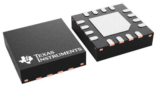
- 3-mm × 3-mm 16-Pin WQFN
TPS65000-Q1에 대한 설명
The TPS65000-Q1 device is a single-chip power-management IC for automotive applications. This device combines a single step-down converter with two low-dropout regulators. The step-down converter enters a low-power mode at light load for maximum efficiency across the widest possible range of load currents. For low-noise applications, the device can be forced into fixed-frequency PWM using the MODE pin. The step-down converter allows the use of a small inductor and capacitors to achieve a small solution size. A power-good status output can be used for sequencing. The LDOs can supply 300 mA, and can operate with an input voltage range from 1.6 V tp 6 V, thus allowing them to be supplied from the step-down converter. The step-down converter and the LDOs have separate voltage inputs and enables, thus allowing for design and sequencing flexibility.
The TPS65000-Q1 is available in a 16-pin leadless package (3-mm × 3-mm WQFN).