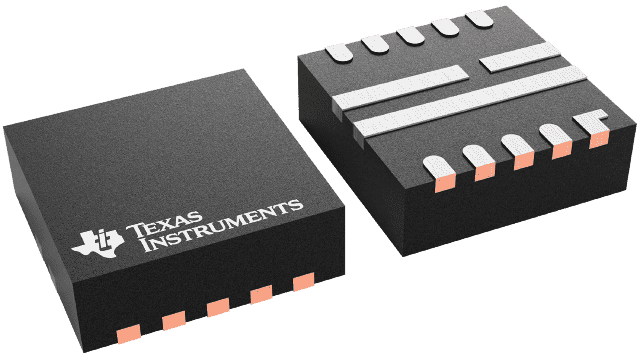
패키징 정보
| 패키지 | 핀 VQFN-HR (RGM) | 13 |
| 작동 온도 범위(°C) -40 to 125 |
| 패키지 수량 | 캐리어 250 | SMALL T&R |
UCD74106의 주요 특징
- Fully Integrated Power Switches With Drivers for Single and Multiphase Synchronous Buck Converters
- Full Compatibility With TI Fusion Digital Power Supply Controllers, (UCD91xx and UCD92xx Families)
- Compatible With Analog Domain Controllers
- Wide Input Voltage Range:
- 4.5 V to 14 V
- Operational Down to 2.2-V Input With an External Bias Supply
- Up to 6-A Output Current
- Operational to 2-MHz Switching Frequency
- Current Limit With Current Limit Flag
- Onboard Regulated 6-V Driver Supply From VIN
- Thermal Protection and Monitoring
UCD74106에 대한 설명
The UCD74106 is a complete power system ready to drive a buck power supply (). High-side MOSFETs, low-side MOSFETs, drivers, current sensing circuitry and necessary protection functions are all integrated into one monolithic solution to facilitate minimum size and maximum efficiency. Driver circuits provide high charge and discharge current for the high-side NMOS switch and the low-side NMOS synchronous rectifier in a synchronous buck circuit. The MOSFET gates are driven to 6.25 V by an internally regulated VGG supply. The internal VGG regulator can be disabled to permit the user to supply an independent gate drive voltage. This flexibility allows a wide power conversion input voltage range of 2.2 V to 18 V. Internal Under Voltage Lockout (UVLO) logic insures VGG is good before allowing chip operation.
A drive logic block allows operation in one of two modes. In synchronous mode, the logic block uses the PWM signal to control both the high-side and low-side gate drive signals. Dead time is optimized to prevent cross conduction. The synchronous rectifier enable (SRE) pin controls whether or not the low-side FET is turned on when the PWM signal is low.
