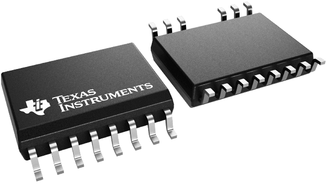
封裝資訊
| 封裝 | 引腳 SOIC (DWK) | 14 |
| 作業溫度範圍 (°C) -40 to 125 |
| 包裝數量 | 運送包裝 2,000 | LARGE T&R |
UCC21530-Q1 的特色
- AEC-Q100 qualified with:
- Device temperature grade 1
- Device HBM ESD classification level H2
- Device CDM ESD classification level C6
- Functional Safety Quality-Managed
- Universal: dual low-side, dual high-side or half-bridge driver
- Wide body SOIC-14 (DWK) package
- 3.3-mm spacing between driver channels
- Switching parameters:
- 19-ns typical propagation delay
- 10-ns minimum pulse width
- 5-ns maximum delay matching
- 6-ns maximum pulse-width distortion
- Common-mode transient immunity (CMTI) greater than 100-V/ns
- Isolation barrier life >40 years
- 4-A peak source, 6-A peak sink output
- TTL and CMOS compatible inputs
- 3-V to 18-V input VCCI range
- Up to 25-V VDD output drive supply
- 8-V and 12-V VDD UVLO options
- Programmable overlap and dead time
- Rejects input pulses and noise transients shorter than 5 ns
- Operating temperature range –40 to +125°C
- Safety-related certifications:
- 8000-VPK isolation per DIN V VDE V 0884-11 :2017-01
- 5.7-kVRMS isolation for 1 minute per UL 1577
- CSA certification per IEC 60950-1, IEC 62368-1, IEC 61010-1 and IEC 60601-1 end equipment standards
- CQC certification per GB4943.1-2011
UCC21530-Q1 的說明
The UCC21530-Q1 is an isolated dual-channel gate driver with 4-A source and 6-A sink peak current. It is designed to drive IGBTs, Si MOSFETs, and SiC MOSFETs up to 5-MHz with best-in-class propagation delay and pulse-width distortion.
The input side is isolated from the two output drivers by a 5.7-kVRMS reinforced isolation barrier, with a minimum of 100-V/ns common-mode transient immunity (CMTI). Internal functional isolation between the two secondary-side drivers allows a working voltage of up to 1850 V.
This driver can be configured as two low-side drivers, two high-side drivers, or a half-bridge driver with programmable dead time (DT). The EN pin pulled low shuts down both outputs simultaneously and allows for normal operation when left open or pulled high. As a fail-safe measure, primary-side logic failures force both outputs low.
The device accepts VDD supply voltages up to 25 V. A wide input VCCI range from 3 V to 18 V makes the driver suitable for interfacing with both analog and digital controllers. All the supply voltage pins have under voltage lock-out (UVLO) protection.
