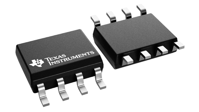
封裝資訊
| 封裝 | 引腳 SOIC (D) | 8 |
| 作業溫度範圍 (°C) -40 to 125 |
| 包裝數量 | 運送包裝 75 | TUBE |
UCC27712 的特色
- High-side and low-side configuration
- Dual inputs with output interlock and 150-ns deadtime
- Fully operational up to 620-V, 700-V absolute maximum on HB pin
- 10-V to 20-V VDD recommended range
- Peak output current 2.8-A sink, 1.8-A source
- dv/dt immunity of 50 V/ns
- Logic operational up to –11 V on HS pin
- Negative voltage tolerance on inputs of –5 V
- Large negative transient safe operating area
- UVLO protection for both channels
- Small propagation delay (100-ns typical)
- Delay matching (12-ns typical)
- Floating channel designed for bootstrap operation
- Low quiescent current
- TTL and CMOS compatible inputs
- Industry standard SOIC-8 package
- All parameters specified over temperature range, –40 °C to +125 °C
UCC27712 的說明
The UCC27712 is a 620-V high-side and low-side gate driver with 1.8-A source, 2.8-A sink current, targeted to drive power MOSFETs or IGBTs.
The recommended VDD operating voltage is 10-V to 20-V for IGBT’s and 10-V to 17-V for power MOSFETs.
The UCC27712 includes protection features where the outputs are held low when the inputs are left open or when the minimum input pulse width specification is not met. Interlock and deadtime functions prevent both outputs from being turned on simultaneously. In addition, the device accepts a wide range bias supply range and offers UVLO protection for both the VDD and HB bias supply.
Developed with TI’s state of the art high-voltage device technology, the device features robust drive with excellent noise and transient immunity including large negative voltage tolerance on its inputs, high dV/dt tolerance, wide negative transient safe operating area (NTSOA) on the switch node (HS), and interlock.
The device consists of one ground-referenced channel (LO) and one floating channel (HO) which is designed for operating with bootstrap or isolated power supplies. The device features fast propagation delays and excellent delay matching between both channels. On the UCC27712, each channel is controlled by its respective input pins, HI and LI.
