SNAS468D September 2008 – December 2014 ADC161S626
PRODUCTION DATA.
- 1 Features
- 2 Applications
- 3 Description
- 4 Revision History
- 5 Pin Configuration and Functions
- 6 Specifications
- 7 Detailed Description
- 8 Application and Implementation
- 9 Power Supply Recommendations
- 10Layout
- 11Device and Documentation Support
- 12Mechanical, Packaging, and Orderable Information
Package Options
Mechanical Data (Package|Pins)
- DGS|10
Thermal pad, mechanical data (Package|Pins)
Orderable Information
7 Detailed Description
7.1 Overview
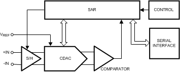
The ADC161S626 is a 16-bit, 50 kSPS to 250 kSPS sampling Analog-to-Digital (A/D) converter. The converter uses a successive approximation register (SAR) architecture based upon capacitive redistribution containing an inherent sample-and-hold function. The differential nature of the analog inputs is maintained from the internal sample-and-hold circuits throughout the A/D converter to provide excellent common-mode signal rejection.
The ADC161S626 operates from independent analog and digital supplies. The analog supply (VA) can range from 4.5 V to 5.5 V and the digital input/output supply (VIO) can range from 2.7 V to 5.5 V. The ADC161S626 utilizes an external reference (VREF), which can be any voltage between 0.5 V and VA. The value of VREF determines the range of the analog input, while the reference input current (IREF) depends upon the conversion rate.
The analog input is presented to two input pins: +IN and –IN. Upon initiation of a conversion, the differential input at these pins is sampled on the internal capacitor array. The inputs are disconnected from the internal circuitry while a conversion is in progress. The ADC161S626 features a zero-power track mode (ZPTM) where the ADC is consuming the minimum amount of power (Power-Down Mode) while the internal sampling capacitor array is tracking the applied analog input voltage. The converter enters ZPTM at the end of each conversion window and experiences no delay when the ADC enters into Conversion Mode. This feature allows the user an easy means for optimizing system performance based on the settling capability of the analog source while minimizing power consumption. ZPTM is exercised by bringing chip select bar (CS) high or when CS is held low after the conversion is complete (after the 18th falling edge of the serial clock).
The ADC161S626 communicates with other devices via a Serial Peripheral Interface (SPI), a synchronous serial interface that operates using three pins: chip select bar (CS), serial clock (SCLK), and serial data out (DOUT). The external SCLK controls data transfer and serves as the conversion clock. The duty cycle of SCLK is essentially unimportant, provided the minimum clock high and low times are met. The minimum SCLK frequency is set by internal capacitor leakage. Each conversion requires a minimum of 18 SCLK cycles to complete. If less than 16 bits of conversion data are required, CS can be brought high at any point during the conversion. This procedure of terminating a conversion prior to completion is commonly referred to as short cycling.
The digital conversion result is clocked out by the SCLK input and is provided serially, most significant bit (MSB) first, at the DOUT pin. The digital data that is provided at the DOUT pin is that of the conversion currently in progress and thus there is no pipe line delay or latency.
7.2 Functional Block Diagram
7.3 Feature Description
7.3.1 Reference Input (VREF)
The externally supplied reference voltage (VREF) sets the analog input range. The ADC161S626 will operate with VREF in the range of 0.5 V to VA.
Operation with VREF below 2.5V is possible with slightly diminished performance. As VREF is reduced, the range of acceptable analog input voltages is reduced. Assuming a proper common-mode input voltage (VCM), the differential peak-to-peak input range is limited to (2 x VREF).
Reducing VREF also reduces the size of the least significant bit (LSB). For example, the size of one LSB is equal to [(2 x VREF) / 2n], which is 152.6 µV where n is 16 bits and VREF is 5V. When the LSB size goes below the noise floor of the ADC161S626, the noise will span an increasing number of codes and overall performance will suffer. Dynamic signals will have their SNR degrade; while, D.C. measurements will have their code uncertainty increase. Since the noise is Gaussian in nature, the effects of this noise can be reduced by averaging the results of a number of consecutive conversions.
VREF and analog inputs (+IN and -IN) are connected to the capacitor array through a switch matrix when the input is sampled. Hence, IREF, I+IN, and I-IN are a series of transient spikes that occur at a frequency dependent on the operating sample rate of the ADC161S626.
IREF changes only slightly with temperature. See the curves, “Reference Current vs. SCLK Frequency” and “Reference Current vs. Temperature” in the Typical Characteristics section for additional details.
7.3.2 Sample and Hold
The ADC161S626 has a differential input where the effective input voltage that is digitized is (+IN) − (−IN).
7.3.2.1 Input Settling
When the ADC161S626 enters acquisition (tACQ) mode at the end of the conversion window, the internal sampling capacitor (CSAMPLE) is connected to the ADC input via an internal switch and a series resistor (RSAMPLE), as shown in Figure 40. Typical values for CSAMPLE and RSAMPLE are 20 pF and 200 ohms respectively. If there is not a large external capacitor (CEXT) at the analog input of the ADC, a voltage spike will be observed at the input pins. This is a result of CSAMPLE and CEXT being at different voltage potentials. The magnitude and direction of the voltage spike depend on the difference between the voltage of CSAMPLE and CEXT. If the voltage at CSAMPLE is greater than the voltage at CEXT, a positive voltage spike will occur. If the opposite is true, a negative voltage spike will occur. It is not critical for the performance of the ADC161S626 to filter out the voltage spike. Rather, ensure that the transient of the spike settles out within tACQ.
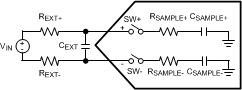 Figure 40. ADC Input Capacitors
7.3.3 Serial Digital Interface
The ADC161S626 communicates via a synchronous 3-wire serial interface as shown in Figure 1 or re-shown in Figure 41 for convenience. CS, chip select bar, initiates conversions and frames the serial data transfers. SCLK (serial clock) controls both the conversion process and the timing of the serial data. DOUT is the serial data output pin, where a conversion result is sent as a serial data stream, MSB first.
A serial frame is initiated on the falling edge of CS and ends on the rising edge of CS. The ADC161S626's DOUT pin is in a high impedance state when CS is high and for the first clock period after CS is asserted; DOUT is active for the remainder of time when CS is asserted.
The ADC161S626 samples the differential input upon the assertion of CS. Assertion is defined as bringing the CS pin to a logic low state. For the first 17 periods of the SCLK following the assertion of CS, the ADC161S626 is converting the analog input voltage. On the 18th falling edge of SCLK, the ADC161S626 enters acquisition (tACQ) mode. For the next three periods of SCLK, the ADC161S626 is operating in acquisition mode where the ADC input is tracking the analog input signal applied across +IN and -IN. During acquisition mode, the ADC161S626 is consuming a minimal amount of power.
The ADC161S626 can enter conversion mode (tCONV) under three different conditions. The first condition involves CS going low (asserted) with SCLK high. In this case, the ADC161S626 enters conversion mode on the first falling edge of SCLK after CS is asserted. In the second condition, CS goes low with SCLK low. Under this condition, the ADC161S626 automatically enters conversion mode and the falling edge of CS is seen as the first falling edge of SCLK. In the third condition, CS and SCLK go low simultaneously and the ADC161S626 enters conversion mode. While there is no timing restriction with respect to the falling edges of CS and SCLK, there are minimum setup and hold time requirements for the falling edge of CS with respect to the rising edge of SCLK. See Figure 5 in the Timing Requirements section for more information.
7.3.3.1 CS Input
The CS (chip select bar) input is active low and is CMOS compatible. The ADC161S626 enters conversion mode when CS is asserted and the SCLK pin is in a logic low state. When CS is high, the ADC161S626 is always in acquisition mode and thus consuming the minimum amount of power. Since CS must be asserted to begin a conversion, the sample rate of the ADC161S626 is equal to the assertion rate of CS.
Proper operation requires that the fall of CS not occur simultaneously with a rising edge of SCLK. If the fall of CS occurs during the rising edge of SCLK, the data might be clocked out one bit early. Whether or not the data is clocked out early depends upon how close the CS transition is to the SCLK transition, the device temperature, and the characteristics of the individual device. To ensure that the MSB is always clocked out at a given time (the 3rd falling edge of SCLK), it is essential that the fall of CS always meet the timing requirement specified in the Timing Requirements table.
7.3.3.2 SCLK Input
The SCLK (serial clock) is used as the conversion clock to shift out the conversion result. SCLK is CMOS compatible. Internal settling time requirements limit the maximum clock frequency while internal capacitor leakage limits the minimum clock frequency. The ADC161S626 offers ensured performance with the clock rates indicated in the electrical table.
The ADC161S626 enters acquisition mode on the 18th falling edge of SCLK during a conversion frame. Assuming that the LSB is clocked into a controller on the 18th rising edge of SCLK, there is a minimum acquisition time period that must be met before a new conversion frame can begin. Other than the 18th rising edge of SCLK that was used to latch the LSB into a controller, there is no requirement for the SCLK to transition during acquisition mode. Therefore, it is acceptable to idle SCLK after the LSB has been latched into the controller.
7.3.3.3 Data Output
The data output format of the ADC161S626 is two’s complement as shown in Figure 42. This figure indicates the ideal output code for a given input voltage and does not include the effects of offset, gain error, linearity errors, or noise. Each data output bit is output on the falling edges of SCLK. DOUT is in a high impedance state for the 1st falling edge of SCLK while the 2nd SCLK falling edge clocks out a leading zero. The 3rd to 18th SCLK falling edges clock out the conversion result, MSB first.
While most receiving systems will capture the digital output bits on the rising edges of SCLK, the falling edges of SCLK may be used to capture the conversion result if the minimum hold time for DOUT is acceptable. See Figure 4 for DOUT hold (tDH) and access (tDA) times.
DOUT is enabled on the second falling edge of SCLK after the assertion of CS and is disabled on the rising edge of CS. If CS is raised prior to the 18th falling edge of SCLK, the current conversion is aborted and DOUT will go into its high impedance state. A new conversion will begin when CS is driven LOW.
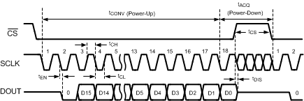 Figure 41. ADC161S626 Single Conversion Timing Diagram
7.4 Device Functional Modes
7.4.1 Differential Input Operation
The transfer curve of the ADC161S626 for a fully differential input signal is shown in Figure 42. A positive full scale output code (0111 1111 1111 1111b or 7FFFh or 32,767d) will be obtained when (+IN) − (−IN) is greater than or equal to (VREF − 1 LSB). A negative full scale code (1000 0000 0000 0000b or 8000h or -32,768d) will be obtained when [(+IN) − (−IN)] is less than or equal to (−VREF + 1 LSB). This ignores gain, offset and linearity errors, which will affect the exact differential input voltage that will determine any given output code.
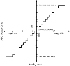 Figure 42. ADC Transfer Curve
Both inputs should be biased at a common mode voltage (VCM), which will be thoroughly discussed in Figure 43 shows the ADC161S626 being driven by a full-scale differential source.
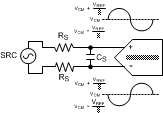 Figure 43. Differential Input
The allowable input common mode voltage (VCM) range depends upon VA and VREF used for the ADC161S626. The ranges of VCM are depicted in Figure 44 and Figure 46. Note that these figures only apply to a VA of 5V. Equations for calculating the minimum and maximum VCM for differential and single-ended operations are shown in Figure 44.
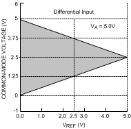 Figure 44. VCM range for Differential Input operation
7.4.2 Single-Ended Input Operation
For single-ended operation, the non-inverting input (+IN) of the ADC161S626 can be driven with a signal that has a peak-to-peak range that is equal to or less than (2 x VREF). The inverting input (−IN) should be biased at a stable VCM that is halfway between these maximum and minimum values. In order to utilize the entire dynamic range of the ADC161S626, VREF is limited to (VA / 2). This allows +IN a maximum swing range of ground to VA. Figure 45 shows the ADC161S626 being driven by a full-scale single-ended source.
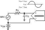 Figure 45. Single-Ended Input
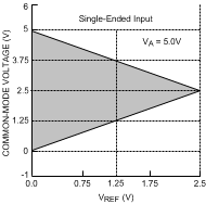 Figure 46. VCM Range for single-Ended Operation
Since the design of the ADC161S626 is optimized for a differential input, the performance degrades slightly when driven with a single-ended input. Linearity characteristics such as INL and DNL typically degrade by 0.1 LSB and dynamic characteristics such as SINAD typically degrade by 2 dB. Note that single-ended operation should only be used if the performance degradation (compared with differential operation) is acceptable.
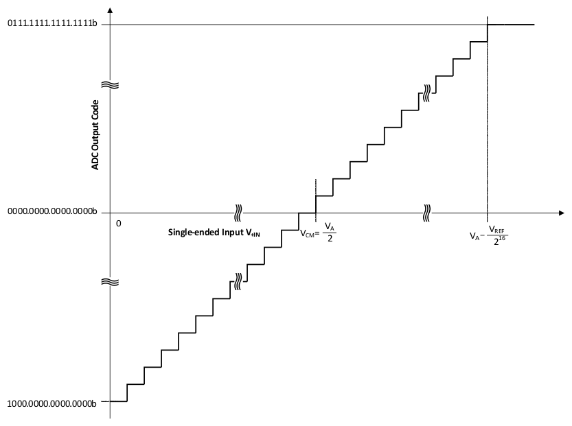 Figure 47. Single-Ended Transfer Characteristic
7.4.3 Short Cycling
Short cycling refers to the process of halting a conversion after the last needed bit is outputted. Short cycling can be used to lower the power consumption in those applications that do not need a full 16-bit resolution, or where an analog signal is being monitored until some condition occurs. In some circumstances, the conversion could be terminated after the first few bits. This will lower power consumption in the converter since the ADC161S626 spends more time in acquisition mode and less time in conversion mode.
Short cycling is accomplished by pulling CS high after the last required bit is received from the ADC161S626 output. This is possible because the ADC161S626 places the latest converted data bit on DOUT as it is generated. If only 10-bits of the conversion result are needed, for example, the conversion can be terminated by pulling CS high after the 10th bit has been clocked out.
7.4.4 Burst Mode Operation
Normal operation of the ADC161S626 requires the SCLK frequency to be 20 times the sample rate and the CS rate to be the same as the sample rate. However, in order to minimize power consumption in applications requiring sample rates below 250 kSPS, the ADC161S626 should be run with an SCLK frequency of 5 MHz and a CS rate as slow as the system requires. When this is accomplished, the ADC161S626 is operating in burst mode. The ADC161S626 enters into acquisition mode at the end of each conversion, minimizing power consumption. This causes the converter to spend the longest possible time in acquisition mode. Since power consumption scales directly with conversion rate, minimizing power consumption requires determining the lowest conversion rate that will satisfy the requirements of the system.