SNAS468D September 2008 – December 2014 ADC161S626
PRODUCTION DATA.
- 1 Features
- 2 Applications
- 3 Description
- 4 Revision History
- 5 Pin Configuration and Functions
- 6 Specifications
- 7 Detailed Description
- 8 Application and Implementation
- 9 Power Supply Recommendations
- 10Layout
- 11Device and Documentation Support
- 12Mechanical, Packaging, and Orderable Information
Package Options
Mechanical Data (Package|Pins)
- DGS|10
Thermal pad, mechanical data (Package|Pins)
Orderable Information
11 Device and Documentation Support
11.1 Device Support
11.1.1 Specification Definitions
-
APERTURE DELAY is the time between the first falling edge of SCLK and the time when the input signal is sampled for conversion.
-
COMMON MODE REJECTION RATIO (CMRR) is a measure of how well in-phase signals common to both input pins are rejected.
To calculate CMRR, the change in output offset is measured while the common mode input voltage is changed from 2V to 3V.
Equation 4. CMRR = 20 LOG ( Δ Common Input / Δ Output Offset)
-
CONVERSION TIME is the time required, after the input voltage is acquired, for the ADC to convert the input voltage to a digital word.
-
DIFFERENTIAL NON-LINEARITY (DNL) is the measure of the maximum deviation from the ideal step size of 1 LSB.
-
DUTY CYCLE is the ratio of the time that a repetitive digital waveform is high to the total time of one period. The specification here refers to the SCLK.
-
EFFECTIVE NUMBER OF BITS (ENOB, or EFFECTIVE BITS) is another method of specifying Signal-to-Noise and Distortion or SINAD. ENOB is defined as (SINAD − 1.76) / 6.02 and says that the converter is equivalent to a perfect ADC of this (ENOB) number of bits.
-
FULL POWER BANDWIDTH is a measure of the frequency at which the reconstructed output fundamental drops 3 dB below its low frequency value for a full scale input.
-
GAIN ERRORis the deviation from the ideal slope of the transfer function. It is the difference between Positive Full-Scale Error and Negative Full-Scale Error and can be calculated as:
Equation 5. Gain Error = Positive Full-Scale Error − Negative Full-Scale Error
-
INTEGRAL NON-LINEARITY (INL) is a measure of the deviation of each individual code from a line drawn from ½ LSB below the first code transition through ½ LSB above the last code transition. The deviation of any given code from this straight line is measured from the center of that code value.
-
MISSING CODES are those output codes that will never appear at the ADC outputs. The ADC161S626 is ensured not to have any missing codes.
-
NEGATIVE FULL-SCALE ERROR is the difference between the differential input voltage at which the output code transitions from code 0x8001h to 0x8000h and −VREF + 1 LSB.
-
NEGATIVE GAIN ERROR is the difference between the negative full-scale error and the offset error.
-
OFFSET ERROR is the difference between the differential input voltage at which the output code transitions from code 0x0000h to 0x0001h and 1 LSB.
-
POSITIVE FULL-SCALE ERRORis the difference between the differential input voltage at which the output code transitions from code 0xFFFEh to 0xFFFFh and VREF - 1 LSB.
-
POSITIVE GAIN ERROR is the difference between the positive full-scale error and the offset error.
-
POWER SUPPLY REJECTION RATIO (PSRR) is a measure of how well a change in the analog supply voltage is rejected. PSRR is calculated from the ratio of the change in offset error for a given change in supply voltage, expressed in dB. For the ADC161S626, VA is changed from 4.5V to 5.5V.
Equation 6. PSRR = 20 LOG (ΔOutput Offset / ΔVA)
-
SIGNAL TO NOISE PLUS DISTORTION (S/N+D or SINAD) is the ratio, expressed in dB, of the rms value of the input signal to the rms value of all of the other spectral components below one-half the sampling frequency, including harmonics but excluding d.c.
-
SIGNAL TO NOISE RATIO (SNR) is the ratio, expressed in dB, of the rms value of the input signal to the rms value of the sum of all other spectral components below one-half the sampling frequency, not including harmonics or d.c.
-
SPURIOUS FREE DYNAMIC RANGE (SFDR)is the difference, expressed in dB, between the desired signal amplitude to the amplitude of the peak spurious spectral component below one-half the sampling frequency, where a spurious spectral component is any signal present in the output spectrum that is not present at the input and may or may not be a harmonic.
-
THROUGHPUT TIMEis the minimum time required between the start of two successive conversion.
-
TOTAL HARMONIC DISTORTION (THD) is the ratio of the rms total of the first five harmonic components at the output to the rms level of the input signal frequency as seen at the output, expressed in dB. THD is calculated as
- Af1 is the RMS power of the input frequency at the output
- Af2 through Af6 are the RMS power in the first 5 harmonic frequencies.
Equation 7. 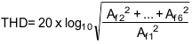
where
11.2 Trademarks
QSPI is a trademark of Motorola.
MICROWIRE is a trademark of National Semiconductor Corp.
All other trademarks are the property of their respective owners.
11.3 Electrostatic Discharge Caution

These devices have limited built-in ESD protection. The leads should be shorted together or the device placed in conductive foam during storage or handling to prevent electrostatic damage to the MOS gates.
11.4 Glossary
SLYZ022 — TI Glossary.
This glossary lists and explains terms, acronyms, and definitions.