SNAS468D September 2008 – December 2014 ADC161S626
PRODUCTION DATA.
- 1 Features
- 2 Applications
- 3 Description
- 4 Revision History
- 5 Pin Configuration and Functions
- 6 Specifications
- 7 Detailed Description
- 8 Application and Implementation
- 9 Power Supply Recommendations
- 10Layout
- 11Device and Documentation Support
- 12Mechanical, Packaging, and Orderable Information
Package Options
Mechanical Data (Package|Pins)
- DGS|10
Thermal pad, mechanical data (Package|Pins)
Orderable Information
5 Pin Configuration and Functions
10 Pins
VSSOP Package
Top View
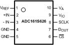
Pin Functions
| PIN | I/O | DESCRIPTION | |
|---|---|---|---|
| NO. | NAME | ||
| 1 | VREF | I | Voltage Reference 0.5 V < VREF < VA |
| 2 | +IN | I | Non-Inverting Input |
| 3 | −IN | I | Inverting Input |
| 4 | GND | Power | Ground |
| 5 | GND | Power | Ground |
| 6 | CS | I | Chip Select Bar |
| 7 | DOUT | O | Serial Data Output |
| 8 | SCLK | I | Serial Clock |
| 9 | VIO | Power | Digital Input/Output Power 2.7 V < VREF < 5.5 V |
| 10 | VA | Power | Analog Power 4.5 V < VREF < 5.5 V |